Single-photon detectors have been in existence for quite some time, but based on non-solid-state form: main examples are photomultiplier tubes (PMTs) and micro-channel plates (MCPs). While these detectors can provide high fill factor and good timing resolution, they have many disadvantages: bulky size, vacuum-based operation, and high price, limiting multi-pixel sensors and also restricting their use to only a few applications. As an alternative to those detectors, solid-state avalanche photodiodes (APDs) operating in normal atmosphere and at room temperature have been developed since the 1960s, but only recently APDs operating in Geiger mode have been demonstrated in standard CMOS technology. The implementation of the devices in standard CMOS technology has enabled integration of electronic circuits on the same silicon chip of the detectors, opening the way to miniaturized, low-cost, and high-volume fabrication of single-photon detectors and sensors.
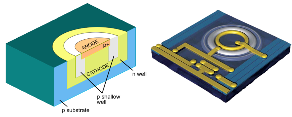
Single-photon avalanche diode (SPADs), also known as Geiger-mode avalanche photodiodes (G-APDs), are solid-state single-photon detectors operating at room temperature capable of capturing single or multiple photons with very high timing resolution, the order of a few tens of picoseconds thanks to the impact ionization mechanism (avalanche multiplication) and the digital nature of its output. While the CMOS SPADs provide many advantages, their performance is still needed to be improved in terms of fill factor (ratio of photon-sensitive area to total area), dark count rate (the rate of spurious pulses due to thermal generation, trap-assisted thermal generation, trap-assisted tunneling, and band-to-band tunneling), photon detection probability (probability that an impinging photon triggers a pulse), timing jitter (uncertainty between actual and measured photon arrival time), afterpulsing probability (probability that an avalanche causes false counts due to traps), etc. In order to improve the performance, the SPAD should be properly simulated and analyzed, (e.g., by means of device modeling, TCAD simulation, etc.) with deep knowledge of physics of semiconductor devices, optoelectronics, and standard semiconductor technology.
The recent availability of the SPADs in standard CMOS technology has paved the way to low-cost, high-volume LiDAR sensors (e.g. advanced driver-assistance systems (ADAS), eventually for autonomous vehicles, drones, robots, machine vision) and mobile phone sensors (e.g. 3D face recognition, gesture recognition), etc. These are also very useful tools in many biomedical and scientific applications, including fluorescence-lifetime imaging microscopy (FLIM), time-of-flight positron emission tomography (TOF PET), super-resolution microscopy, near infrared imaging (NIRI), time-resolved Raman spectroscopy, random-number generator, etc. It can be also utilized in more applications wherever single-photon sensitivity and high precision time-of-arrival detection are critical.
Relevant publications
E. Charbon, “Single-photon imaging in complementary metal oxide semiconductor processes,” Phil. Trans. R. Soc. A, vol. 372, Feb. 2014, Art. no. 20130100.
C. Bruschini et al., “Ten years of biophotonics single-photon SPAD imager applications – retrospective and outlook,” Proc. SPIE, vol. 10069, Feb. 2017, Art. no. 100691S.
M.-J. Lee et al., “High-Performance Back-Illuminated Three-Dimensional Stacked Single-Photon Avalanche Diode Implemented in 45-nm CMOS Technology,” IEEE J. Sel. Top. Quantum Electron., vol. 24, no. 6, Nov./Dec. 2018. Art. no. 3801809.