Project completed
Ge-on-Si Single Photon Avalanche Diode Working at Near-Infrared Wavelength
Progressing of sensors and their applications has become essential to address some major challenges of today’s society such as monitoring and control of our environment and the quality of life. In recent years, semiconductor-based sensors for gases and liquids detection have experienced a great development. These devices have the benefit of relatively cheap manufacturing, while they suffer from limited sensitivity. To improve the sensitivity of devices, developing optical-based sensors have a strong demand. Optical absorption techniques offer the possibility to realize a non-invasive and highly sensitive detection platform for both gases and liquids. Most of the required frequencies for targeted molecules are located in the near and mid-infrared range. In near-infrared range, most of the current researches are focused on Germanium as a good absorbing material option. The advantage of this material is its compatibility with Silicon and standard CMOS processes as well as its much higher absorption coefficient compared to Si. The available SiGe photodetectors based on their structures and bias levels exhibit various sensitivity and efficiency. The best proposed SiGe photodetector working in near breakdown voltage has the gain of 65, while the gain of SPAD photodetectors is theoretically infinitive. This PhD project will present a new generation of single photon avalanche diodes (SPAD) working in near-infrared range. The Ge-based SPAD photodetectors have the advantages of high sensitivity and time resolution; this type of detector exhibits capability of single photon sensitivity. By biasing a photodiode above the breakdown voltage, Geiger mode, a large avalanche current is generated and resulted in a virtually infinite optical gain.

SPAD test circuit
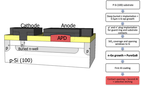
The fabrication process of the SiGe SPAD consists of a standard CMOS process and probably post-processing steps for growing Ge on top of Si/SiO2. For preventing the premature breakdown in our devices, guard ring layers will be considered in their structure designs. Also, for carrying lights from a source to detectors, planar Si waveguides will be designed. This approach can also improve the speed and quantum efficiency of the SiGe photodetector. On the other hand, one of the drawbacks of using Ge on top of Si is the lattice mismatch between them resulted in high dark current. We will have cooperation with some groups working on this problem to improve the Ge growing methods and our designed structure will be fabricated with these new methods. Whereas a good Ge growing method can reduce dark current, the complexity of read-out devices will be decreased.
Keywords: Single photo avalanche diode, SPAD, SiGe SPAD, SPAD array, Near-Infrared, CMOS compatible, Si/SiO2 Waveguide

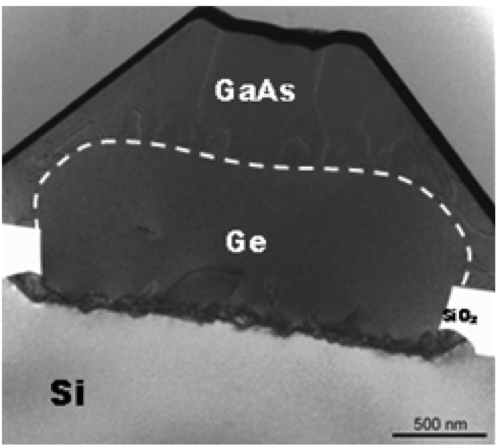
Cross-sectional TEM image of a Ge-island epitaxially grown at 700ºC on patterned Si followed by in-situ growth of a GaAs layer. Due to the rounded form of the Ge surface, the GaAs growth is not entirely free of dislocations [1].

CMOS Compatible process flow of Ge APD fabrication, [1]
References:
[1]. “A CMOS Compatible Ge-on-Si APD Operating in Proportional and Geiger Modes at Infrared Wavelengths,” A. Sammak, M. Aminian, L. Qi, W. B. de Boer, E. Charbon and L. K. Nanver, IEDM 2011.
[2]. “A Ge-on-Si Single Photon Avalanche Diode Operating in Geiger Mode at Infrared Wavelengths,” M. Aminian, A. Sammak, L. K. Nanver, and E. Charbon, SPIE Defense, Security, and Sensing 2012.
Aknowledgment:
This project has received financial support from the NanoTera-IrSens project. Also, we would like to thank the staff of the DIMES cleanrooms and measurement room.