We develop integrated photonic devices for classical and quantum terahertz science. We design on-chip components in various material platforms to enhance the interaction between terahertz and optical photons.
Terahertz transmission lines
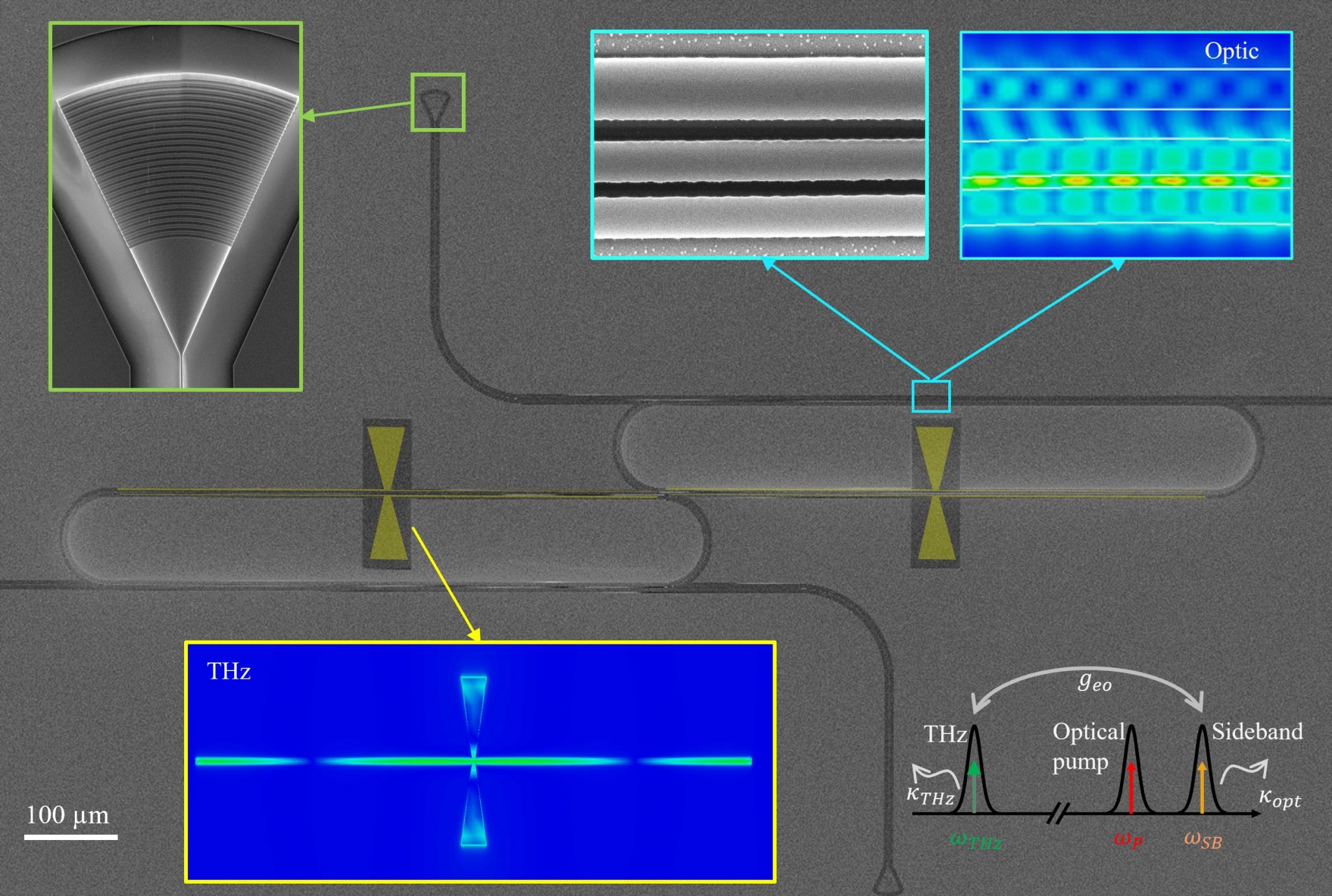
A key component of our devices are terahertz transmission lines that we pattern around optical waveguides as shown below for example on a lithium niobate chip.

These enable phase matching between the terahertz and optical fields, similar to the design concept used in broadband electro-optic modulators. This allows to efficiently generate, guide and store terahertz signals on the same chip as integrated photonic circuits – over the very large frequency range from 200 GHz to 3.5 THz that are else covered only by very distinct and incompatible technologies (multiplier chains up to 1 THz, quantum cascade lasers above 1.9 THz).

By terminating the transmission lines with an open end, we can even realize terahertz cavities, which are beneficial for field enhancement.
Terahertz antennas
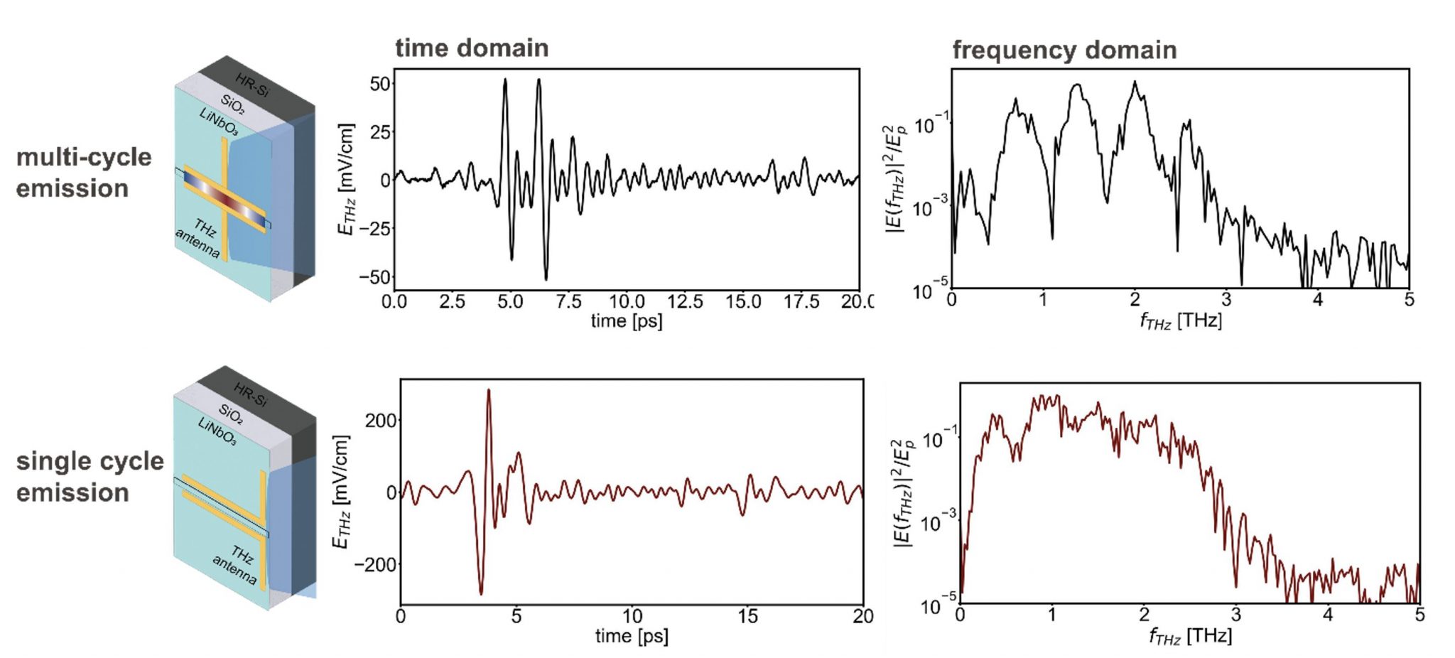
A second knob relies on developing successful strategies to couple terahertz fields in and out these on-chip transmission lines. This can be achieved in a very small form factor by terminating the transmission lines with printed antennas. The geometrical dimensions of the antenna determine its operating frequency and bandwidth. In the picture below we see a simple dipolar antenna patterned at the end of the transmission line.
 |
 |
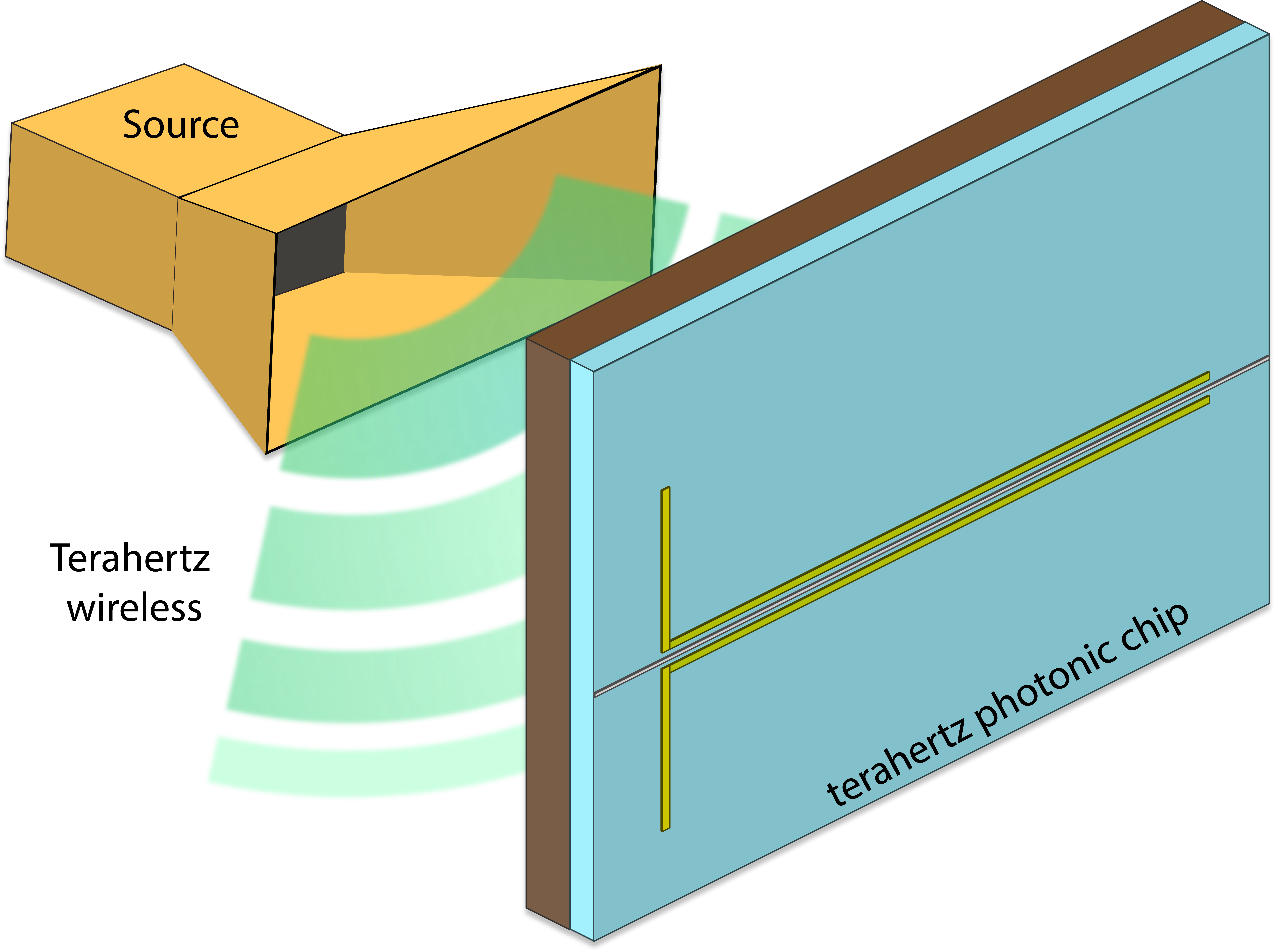
This allows to efficiently couple free space terahertz radiation which may come from a source into the terahertz waveguide.
Cavity-based electro-optics
A third knob relies on the utilization of electro-optic cavities, and then integrating emerging nonlinear optical materials with exceptionally high electro-optic coefficients onto photonic chips. This integration will involve the meticulous design and fabrication of optical and THz cavities to enhance field confinement while minimizing losses. Two strategies are proposed to overcome limitations in efficiency at high frequencies: 1) optimizing THz cavity design, and 2) utilizing low-loss metals to mitigate losses in THz integrated circuits.

Altogether, these efforts seek to address two enduring challenges:
1) enhancing the efficiency of photonic integrated circuits employing electro-optic (Pockels) effects,
2) overcoming obstacles at high frequencies in the THz gap, demonstrating signal generation and detection beyond 100 GHz on a photonic chip.
This research not only aim to realize powerful chip-scale platform for fundamental research at high frequencies, but also anticipates advancements in sensing capabilities within the THz domain. The transformative impact extends to various applications, including wireless communication, LiDAR, non-invasive imaging, and quantum technologies.