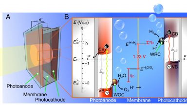
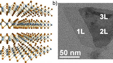
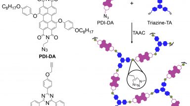
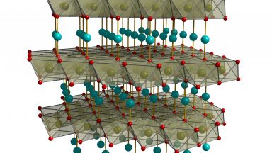
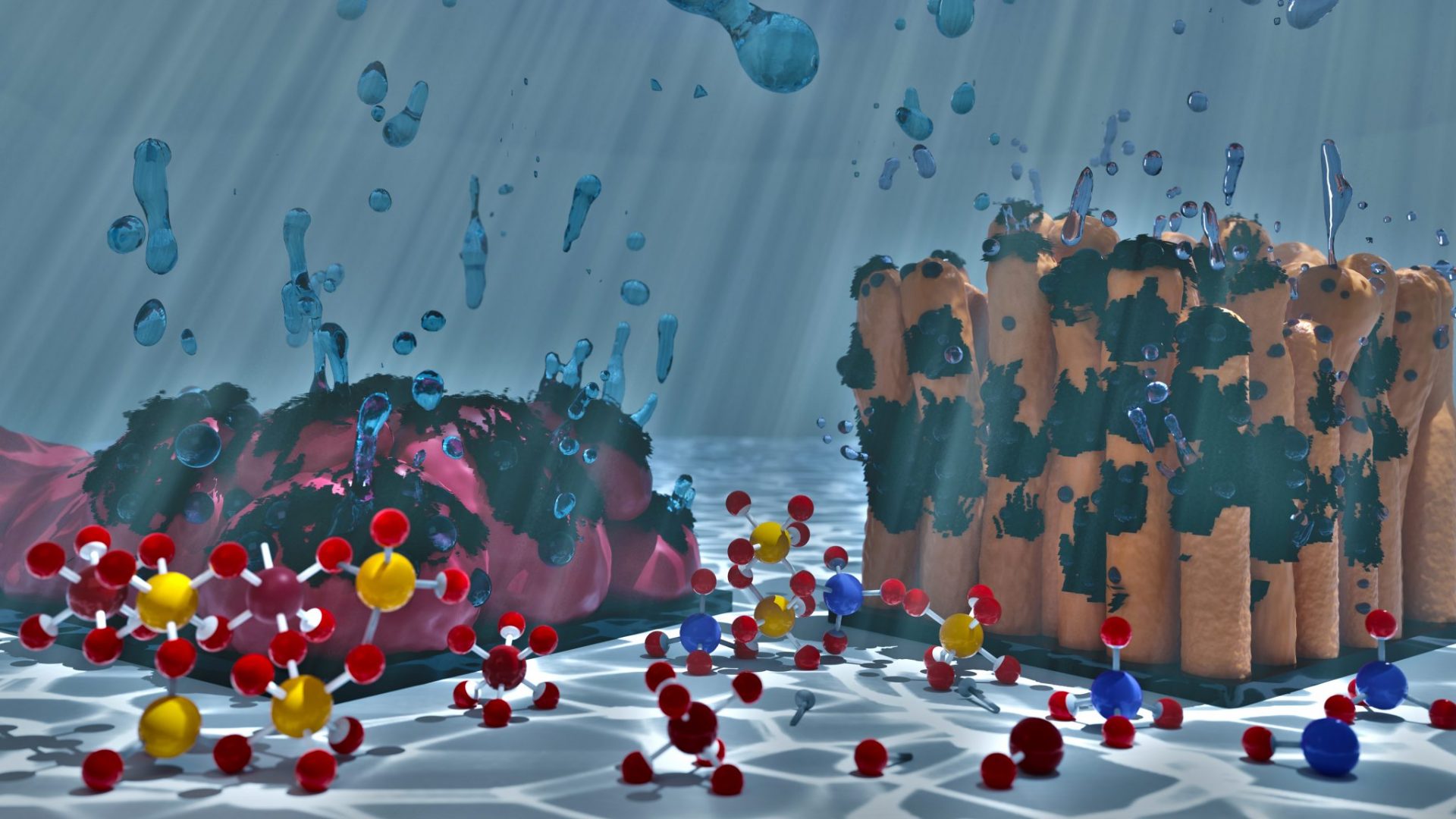
Today’s traditional electronic devices are based on crystalline semiconductors, like silicon, that require strict control over material purity and crystallinity making them difficult and costly to synthesize. Moreover, functional structures of crystalline semiconductor devices are prepared today by “top-down” methodologies. These conditions necessitate complicated fabrication procedures and lead to expensive products that are difficult to prepare at large scale. We envision that tomorrow’s devices will be fabricated with simple and inexpensive solution-based printing techniques and “bottom-up” self-assembly of functional structures. Attaining this goal will provide access to low-cost, large area and flexible displays, sensors and solar cells. However, the development of semiconducting materials that can be solution-processed and self-assembled into functional thin-films at low temperature, while simultaneously providing excellent device characteristics, represents a significant challenge for materials chemists and engineers. Our research is directed to engineering new, inexpensive, and solution-processable semiconductor materials and implementing them into high performance devices. We are especially driven by the goal of inexpensive solar energy conversion. As such, we focus on materials systems with sufficient earth abundance and environmental compatibility, and we employ techniques that are highly scalable and economically feasible. LIMNO incorporates competences of semiconductor synthesis, characterization, and device fabrication while individual projects concentrate on directing the composition, crystallinity, self-assembly, and morphology of our new materials using bottom-up techniques in order to control the semiconductor band gap, light absorption, charge transfer, carrier transport and device performance.
