Polycrystalline alumina (PCA) is a promising and economic replacement for sapphire for various applications ranging from biomedicine to solar energy. In addition to the thickness, its optical properties are very sensitive to the microstructure: the grain size and the residual porosity are the most important parameters.
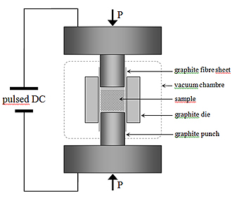
Spark plasma sintering (SPS, Prof. Zhao Zhe, KTH, Stockholm Sweden) has been used giving excellent sintering results. A systematic experimental design was used to study Mg, Y and La single or co-doping and the sintering pressure and temperature on the transmittance of alumina produced by SPS. Different green body fabrication and powder processing methods have been investigated (Dry Processing).
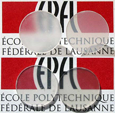
So far real-inline transmittances (RIT) of > 50% (best 57%) could be reached for almost any combination of the studied dopants at 255 and 450 ppm cationic ratio after experimental optimisation.
 |
 |
|
| Schematic representation of an SPS sintering machine | PCA samples with RIT’s: left: 8.7%, right: 57% 1.5 cm above and posed on the sheet respectively |
FIB-Nanotomography and optical modelling of transparent alumina ceramics.
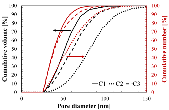
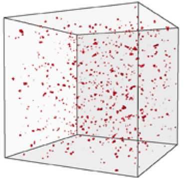
Researchers at the Powder Technology Laboratory (P. Bowen and M. Stuer) and the Center for Electron Microscopy (M. Cantoni, Prof. C. Hebert) have made a significant breakthrough in the optical modelling of transparent polycrystalline alumina (PCA) using nanoscale 3D FIB tomography. Previous models of both grain boundary and pore scattering were developed without sufficient experimental corroboration. A first direct link between the observed transparency, defect size and porosity, was established using novel experimental full 3D pore reconstruction from the FIB tomography.
 |
 |
|
| 3D-FIB pore size distributions for 3 samples with different transmittances C1-RIT 49%, C2-RIT 10% and C3-RIT 45% | The 3D-FIB pore reconstruction of a volume of 4.11 x 4.11 x 4.11 μm of sample C1 |
The new theoretical model developed in collaboration with C. Pecharroman (Instituto de Ciencia de Materiales de Madrid, CSIC) showed how the previous model was erroneous by an order of magnitude. These exciting experimental and new theoretical results correctly identified for the first time the relative contributions of different scattering mechanisms. This now paves the way forward for microstructural tuning of transparent polycrystalline alumina for a multitude of applications.
STEM-EDX Spectroscopy of Grain Boundaries
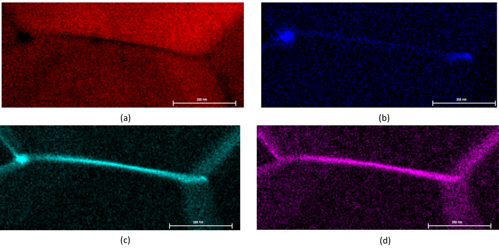
Microstructural characterizations of Y-La codoped α-alumina samples with elemental analysis were carried out in collaboration with the center for electron microscopy (CIME) at EPFL in order to validate the atomistic modelling results. Microscopy results confirmed the simultaneous segregation of both the dopants on all grain boundaries as predicted by the atomistic simulations.
 |
|
| STEM-EDX spectroscopy results showing the presence of dopants and impurities at a grain boundary: (a) Aluminium, (b) Chlorine, (c) Lanthanum and (d) Yttrium. |
Publications:
M. Stuer et al. Adv. Funct. Materials. 22(11) 2303-2309 (2012)