


2025
Additive manufacturing of water-soluble 3D micro molds for complex-shaped lipid microparticles
Nature communications. 2025. Vol. 16, num. 1. DOI : 10.1038/s41467-025-56984-7.Superconducting microwave oscillators as detectors for ESR spectroscopy
Applied Physics Letters. 2025. Vol. 126, num. 15, p. 154101. DOI : 10.1063/5.0260098.Addition of a tubular collector to a MEWron melt electrowriting printer
2025
Impact of Simple Parameters on Fibre Diameter in Melt Electrowriting (MEW)
2025.Fused Deposition Modelling and Melt Electrowriting of Metallic Tubes
2025.Microfabrication of lipids for drug delivery applications
Lausanne, EPFL, 2025.Single chip microsystems for electron spin resonance spectroscopy and inductive proximity sensing
Lausanne, EPFL, 2025.2024
Devices for the electrical stimulation of the olfactory system: A review
Biosensors and Bioelectronics. 2024. Vol. 271. DOI : 10.1016/j.bios.2024.117063.MixedLAB: Mixed Reality to Teach Students Experimental Knowledge in Microfabrication
2024. 52nd Annual Conference of the European Society for Engineering Education, Lausanne, Switzerland, 2024-09-02-2024-09-05. DOI : 10.5281/zenodo.14256909.Element-specific X-Ray detection of electron paramagnetic resonance in thin films of quantum bits
Nature communications. 2024. Vol. 15, num. 1. DOI : 10.1038/s41467-024-54586-3.200 GHz single chip microsystems for dynamic nuclear polarization enhanced NMR spectroscopy
Nature communications. 2024. Vol. 15, num. 1. DOI : 10.1038/s41467-024-49767-z.Deterministic grayscale nanotopography to engineer mobilities in strained MoS2 FETs
Nature communications. 2024. Vol. 15, num. 1. DOI : 10.1038/s41467-024-51165-4. Conversion of a Voron FDM printer to a MEWron melt electrowriting printer
2024
Ultraviolet to mid-infrared optical properties of sputtered Al(Sc)N-on-SiO2 thin films and experimental demonstration of AlN integrated photonic devices in the telecom C-band
Optics Express. 2024. Vol. 32, num. 24, p. 42529 – 42544. DOI : 10.1364/OE.540975. Laser-Induced Forward Transfer of SU-8 Microdisks as Carriers of Metallic Microdevices
JOURNAL OF MICROELECTROMECHANICAL SYSTEMS. 2024. DOI : 10.1109/JMEMS.2024.3487248.Towards standardisation of parameter reporting for melt electrowriting
2024
Performance Comparison of Shape Memory Polymer Structures Printed by Fused Deposition Modeling and Melt Electrowriting
Advanced Materials Technologies. 2024. DOI : 10.1002/admt.202400466.X-Band Single Chip Integrated Pulsed Electron Spin Resonance Microsystem
Analytical Chemistry. 2024. DOI : 10.1021/acs.analchem.4c02769.Hot topic: Mapping of the human intranasal mucosal thermal sensitivity: A clinical study on thermal threshold and trigeminal receptors
PloS one. 2024. Vol. 19, num. 8 August. DOI : 10.1371/journal.pone.0304874.Additive manufacturing of novel tubular designs using a filament-driven opensource melt electrowriting machine
Swiss e-print, Dübendorf, Switzerland, 2024-09-25 – 2024-09-26.All-Printed Finger-Inspired Tactile Sensor Array for Microscale Texture Detection and 3D Reconstruction
Advanced science (Weinheim, Baden-Wurttemberg, Germany). 2024. Vol. 11, num. 26. DOI : 10.1002/advs.202400479.Resist-free metal patterning inside 3D printed concave tubular structures using a flexible stencil
50th International Micro and Nano Engineering Conference, Montpellier, France, 2024-09-16 – 2024-09-19.Development of core-shell lipid microneedles for sublingual delivery
2024.Designing of Bridges on Stencils: Calculation and Simulation
2024.Melt Electro-Writing for Wound Repair and Drug Delivery with Lipid Medium
2024.Electrowriting of SU-8 Microfibers
Polymers. 2024. Vol. 16, num. 12. DOI : 10.3390/polym16121630.Semester Project Report (2024 Spring) Grayscale thermal scanning probe lithography in photonic applications
2024.[n]Cycloparaphenylenes as Compatible Fluorophores for Melt Electrowriting
Small. 2024. DOI : 10.1002/smll.202400882.A continuous-wave and pulsed X-band electron spin resonance spectrometer operating in ultra-high vacuum for the study of low dimensional spin ensembles
Review Of Scientific Instruments. 2024. Vol. 95, num. 6, p. 063904. DOI : 10.1063/5.0189974.Near-Room-Temperature Detection of Aromatic Compounds with Inkjet-Printed Plasticized Polymer Composites
Acs Sensors. 2024. Vol. 9, num. 3, p. 1382 – 1390. DOI : 10.1021/acssensors.3c02406.First Advanced Bilayer Scaffolds for Tailored Skin Tissue Engineering Produced via Electrospinning and Melt Electrowriting
Advanced Functional Materials. 2024. DOI : 10.1002/adfm.202314757.Microstructured plastic scintillators for pencil beam profiling in proton-therapy accelerators
Nuclear Instruments and Methods in Physics Research Section A: Accelerators, Spectrometers, Detectors and Associated Equipment. 2024. Vol. 1062, p. 169176. DOI : 10.1016/j.nima.2024.169176.Tomographic microscopy of functionally graded polymer-derived SiCN ceramics with tunable gradients
Materialia. 2024. Vol. 33, p. 102025. DOI : 10.1016/j.mtla.2024.102025.Optical Ring Resonators in Sputtered Aluminum Nitride on Insulator for Integrated Photonic MEMS
2024. International Conference on Optical MEMS and Nanophotonics, San Sebastian, Spain, 2024-07-28 – 2024-08-01. DOI : 10.1109/OMN61224.2024.10685232.2023
Towards optical MAS magnetic resonance using optical traps
Journal Of Magnetic Resonance Open. 2023. Vol. 18, p. 100145. DOI : 10.1016/j.jmro.2023.100145.Melt Electrowriting Report
2023.Effects of Electrode Design on the Melt Electrowriting of Sinusoidal Structures
Advanced Engineering Materials. 2023. DOI : 10.1002/adem.202300335.Liquid-in-a-MEMS: Encapsulation of Liquid in a Microcapsule by Inkjet Printing
2023.LIQUID-IN-A-MEMS: ENCAPSULATION OF LIQUID IN A MICROCAPSULE BY INKJET PRINTING
2023. 22nd International Conference on Solid-State Sensors, Actuators and Microsystems, Kyoto, Japan, 2023-06-25 – 2023-06-29.Fabrication and Characterization of Lipid Sublingual Drug Delivery Device
2023.Designing Mixed Reality Experiences for Microfabrication Training
2023.Nanoimprint stamp fabrication by combination of T-SPL and dry etching
2023.Nanoliter Liquid Packaging in a Bioresorbable Microsystem by Additive Manufacturing and its Application as a Controlled Drug Delivery Device
Advanced Functional Materials. 2023. num. 2302385. DOI : 10.1002/adfm.202302385.MEWron: An open-source melt electrowriting platform
Additive Manufacturing. 2023. Vol. 71, p. 103604. DOI : 10.1016/j.addma.2023.103604.Biodegradable Implantable Microsystems
2023. 2022 International Electron Devices Meeting (IEDM), San Francisco, CA, USA, December 3-7, 2022. p. 29.4.1 – 29.4.4. DOI : 10.1109/IEDM45625.2022.10019376.One-step fabrication of high refractive index inorganic nanostructures
Journal Of Sol-Gel Science And Technology. 2023. Vol. 107, p. 122 – 132. DOI : 10.1007/s10971-021-05633-8.Single Chip Dynamic Nuclear Polarization Microsystems
Lausanne, EPFL, 2023.Laser-Induced Forward Transfer of Functional Microdevices
Lausanne, EPFL, 2023.Grayscale Nanopatterning by Thermal Scanning Probe Lithography
2023.2022
Fabrication of Lipid Microstructure for Oral Drug Delivery Device
2022.Nanobridge Stencil Enabling High Resolution Arbitrarily Shaped Metallic Thin Films on Various Substrates
Advanced Materials Technologies. 2022. DOI : 10.1002/admt.202201119.Comparison of electrical and optical transduction modes of DNA-wrapped SWCNT nanosensors for the reversible detection of neurotransmitters.
Biosensors & Bioelectronics. 2022. Vol. 216, p. 114642. DOI : 10.1016/j.bios.2022.114642.Edge-Contact MoS2 Transistors Fabricated Using Thermal Scanning Probe Lithography
ACS Applied Materials & Interfaces. 2022. Vol. 14, num. 37, p. 42328 – 42336. DOI : 10.1021/acsami.2c10150.Nanopore Generation in Biodegradable Silk/Magnetic Nanoparticle Membranes by an External Magnetic Field for Implantable Drug Delivery
ACS Applied Materials & Interfaces. 2022. Vol. 14, num. 35, p. 40418 – 40426. DOI : 10.1021/acsami.2c10603.Multiscale microshaping of functionally graded polymer-derived SiCN ceramics
Ceramics in Europe 2022, Krakow, Poland, 10th – 14th July, 2022.Nanofabrication of hard mask for single dopant-based quantum hardware
2022.Ion Implantation for Single Dopant Based Quantum Hardware
2022.Melt Electrowriting of Lipids for drug delivery
2022.Liquid encapsulated drug delivery device for acoustically-controlled release
2022.Study of the enhanced electricity output of a sliding droplet-based triboelectric nanogenerator for droplet sensor design
Nano Energy. 2022. Vol. 98, p. 107166. DOI : 10.1016/j.nanoen.2022.107166.SU-8 cantilever with integrated pyrolyzed glass-like carbon piezoresistor
Microsystems & Nanoengineering. 2022. Vol. 8, num. 1, p. 22. DOI : 10.1038/s41378-022-00351-9.Precise Capillary‐Assisted Nanoparticle Assembly in Reusable Templates
Particle & Particle Systems Characterization. 2022. p. 1 – 8, 2100288. DOI : 10.1002/ppsc.202100288.NMR spectroscopy of a single mammalian early stage embryo
Journal of Magnetic Resonance. 2022. Vol. 335, p. 107142. DOI : 10.1016/j.jmr.2021.107142.Multiscale 2D/3D microshaping of property-contrast polymer-derived SiCN
46th International Conference and Expo on Advanced Ceramics and Composites (ICACC2022), Virtual, January 24-28, 2022.Tomographic Volumetric Additive Manufacturing of Silicon Oxycarbide Ceramics
Advanced Engineering Materials. 2022. Vol. 24, num. 7, p. 2101345. DOI : 10.1002/adem.202101345.Multiscale microshaping of functionally graded polymer-derived SiCN ceramics
Lausanne, EPFL, 2022.SPONTANEOUS FORMATION AND PROGRAMMABLE ORIENTATION OF SURFACE WRINKLES ON THERMOSENSITIVE RESIST
2022
FABRICATION OF TRANSFERRED FLEXIBLE PMMA STENCIL LITHOGRAPHY
2022
Development of stencil lithography for stretchable interconnects
Lausanne, EPFL, 2022.Experimental Analysis of Ductile Cutting Regime in Face Milling of Sintered Silicon Carbide
Materials. 2022. Vol. 15, num. 7, p. 2409. DOI : 10.3390/ma15072409.Scalable fabrication of functional nanostructures on stretchable substrates by capillary-assisted particle assembly and adhesion lithography
Lausanne, EPFL, 2022.Developing Melt Electrowriting on an Open-Source Fused Filament Fabrication Platform
2022.2021
Multiscale 2D/3D microshaping and property tuning of polymer-derived SiCN ceramics
Journal of the European Ceramic Society. 2021. Vol. 42, num. 5, p. 1963 – 1970. DOI : 10.1016/j.jeurceramsoc.2021.12.044.Stretchable Conductors Fabricated by Stencil Lithography and Centrifugal Force-Assisted Patterning of Liquid Metal
ACS Applied Electronic Materials. 2021. Vol. 3, num. 12, p. 5423 – 5432. DOI : 10.1021/acsaelm.1c00884.Spontaneous formation of ordered micro-wrinkles on a thermosensitive resist
47th Micro and Nano Engineering Conference (MNE 2021), Turin, Italy, September 20-23, 2021.High resolution meandering metal patterns enabled by nano-bridge stencil
47th international Conference on Micro and Nano Engineering (MNE2021), Turin, Italy, September 20-23, 2021.Freeform Microstructuring of Cast Polymer-Derived Ceramics by Sacrificial Direct Laser Writing
47th international Conference on Micro and Nano Engineering (MNE2021), Turin, Italy, September 20-23, 2021.Laser-induced forward transfer of functional SU-8 microparts
47th international Conference on Micro and Nano Engineering (MNE2021), Turin, Italy, September 20-23, 2021.Edge-contact MoS2 transistors made by thermal scanning probe lithography
Micro and Nano Engineering Conference, Turin, Italy, September 20th – 23rd, 2021.Precise Capillary-Assisted Nanoparticle assembly in Reusable Templates
47th Micro and Nano Engineering Conference (MNE 2021), Turin, Italy, September 20-23, 2021.A Low Power 35 GHz HEMT Oscillator for Electron Spin Resonance Spectroscopy
2021. 2021 IEEE Radio Frequency Integrated Circuits Symposium (RFIC), Atlanta, GA, USA, June 7-9, 2021. p. 19 – 22. DOI : 10.1109/RFIC51843.2021.9490487.Thermal scanning probe lithography for 2D material-based gas sensing
2021.Optimization of MEW instrument components and their assembly
2021.Fabrication of biocompatible metallic structures on biodegradable polymer films by stencil lithography
2021.Recent progress in silk fibroin-based flexible electronics
Microsystems & Nanoengineering. 2021. Vol. 7, num. 1, p. 35. DOI : 10.1038/s41378-021-00261-2.Next Generation Cell Culture Tools Featuring Micro- and Nanotopographies for Biological Screening
Advanced Functional Materials. 2021. p. 2100881. DOI : 10.1002/adfm.202100881.Printed Polymer Composite Sensors for Low-Power, Near Room-Temperature Detection and Classification of VOCS
2021. 34th International Conference on Micro Electro Mechanical Systems (IEEE MEMS 2021), Gainesville, FL, USA (virtual event), January 25-29, 2021. p. 274 – 277. DOI : 10.1109/MEMS51782.2021.9375208.Precision Surface Microtopography Regulates Cell Fate via Changes to Actomyosin Contractility and Nuclear Architecture
Advanced Science. 2021. Vol. 8, num. 6, p. 2003186. DOI : 10.1002/advs.202003186.Capillary assisted particle assembly for high aspect ratio nanorods
2021.2D material-based gas sensing device
2021.PDC microfabrication through KOH-etched Si mould casting
2021.Experimental study of the strain patterned in 2D materials using thermal nanoimprint lithography
2021.Microfabricated nanomotion detectors for rapid cells viability tests
Lausanne, EPFL, 2021.Inkjet-printed polymer composites for the detection of volatile organic compounds
Lausanne, EPFL, 2021.A Glass-Like Carbon Mems Strain Sensor
2021. 21st International Conference on Solid-State Sensors, Actuators and Microsystems (Transducers), ELECTR NETWORK, Jun 20-25, 2021. p. 871 – 874. DOI : 10.1109/TRANSDUCERS50396.2021.9495726.Thermomechanical nanocutting and nanostraining of 2D materials
Heidelberg Instruments NanoFrazor Webinar series, 2021-02-09.Hierarchical Micromold Structuring via 2PP Micro-Stereolithography
2021.2020
Inkjet‐Printed Composites for Room‐Temperature VOC Sensing: From Ink Formulation to Sensor Characterization
Advanced Materials Technologies. 2020. p. 1 – 11, 2000929. DOI : 10.1002/admt.202000929.Electrochemical performance of polymer-derived SiOC and SiTiOC ceramic electrodes for artificial cardiac pacemaker applications
Ceramics International. 2020. Vol. 47, num. 6, p. 7593 – 7601. DOI : 10.1016/j.ceramint.2020.11.098.Designs and Characterization of Subunit Ebola GP Vaccine Candidates: Implications for Immunogenicity
Frontiers In Immunology. 2020. Vol. 11, p. 586595. DOI : 10.3389/fimmu.2020.586595.NMR microsystem for label-free characterization of 3D nanoliter microtissues
Scientific Reports. 2020. Vol. 10, p. 1 – 9, 18306. DOI : 10.1038/s41598-020-75480-0.Thermomechanical Nanostraining of Two-Dimensional Materials
Nano Letters. 2020. Vol. 20, num. 11, p. 8250 – 8257. DOI : 10.1021/acs.nanolett.0c03358.Reversible Drug Delivery: Thermal and pH Sensitive Composite Membrane for On‐Demand Drug Delivery by Applying an Alternating Magnetic Field (Adv. Mater. Interfaces 17/2020)
Advanced Materials Interfaces. 2020. Vol. 7, num. 17, p. 2070095. DOI : 10.1002/admi.202070095.On the effect of linear feedback and parametric pumping on a resonator’s frequency stability
New Journal Of Physics. 2020. Vol. 22, num. 9, p. 093049. DOI : 10.1088/1367-2630/abb1dd.Electrical Conductivity Tuning of Polysilazane-Derived Silicon Carbonitride Ceramics
Electroceramics XVII, Online (Darmstadt, Germany), Août 24-27, 2020.Analysis of volumetric mass transfer coefficient (k(L)a) in small- (250 mL) to large-scale (2500 L) orbitally shaken bioreactors
3 Biotech. 2020. Vol. 10, num. 9, p. 397. DOI : 10.1007/s13205-020-02352-9.Cracks, porosity and microstructure of Ti modified polymer-derived SiOC revealed by absorption-, XRD- and XRF-contrast 2D and 3D imaging
Acta Materialia. 2020. Vol. 198, p. 134 – 144. DOI : 10.1016/j.actamat.2020.07.067.Simulation of silicon KOH and dry etching methods for micromould fabrication
2020.Review on Crystallization and Phase Change of Low-Dimensional Materials Using Thermal Probes
2020.Part I. Effect of plasticizer on the sensing performance of inkjet-printed PVP/CB composite Part II. Nanostructuring of 2D materials for improved gas sensing performance
2020.Review of Liquid-Solid Triboelectric Generator
2020.Microfabrication on bioresorbable materials
2020.Thermal and pH Sensitive Composite Membrane for On-Demand Drug Delivery by Applying an Alternating Magnetic Field
Advanced Materials Interfaces. 2020. Vol. 7, num. 17, p. 2000733. DOI : 10.1002/admi.202000733.The Delivery of alpha 1-Antitrypsin Therapy Through Transepidermal Route: Worthwhile to Explore
Frontiers In Pharmacology. 2020. Vol. 11, p. 983. DOI : 10.3389/fphar.2020.00983.Immobilization of single-walled carbon nanotubes by dielectrophoresis using a microfluidic channel
2020.Single chip dynamic nuclear polarization microsystem
Analytical Chemistry. 2020. Vol. 92, num. 14, p. 9782 – 9789. DOI : 10.1021/acs.analchem.0c01221.Thermomechanical Nanocutting of 2D Materials
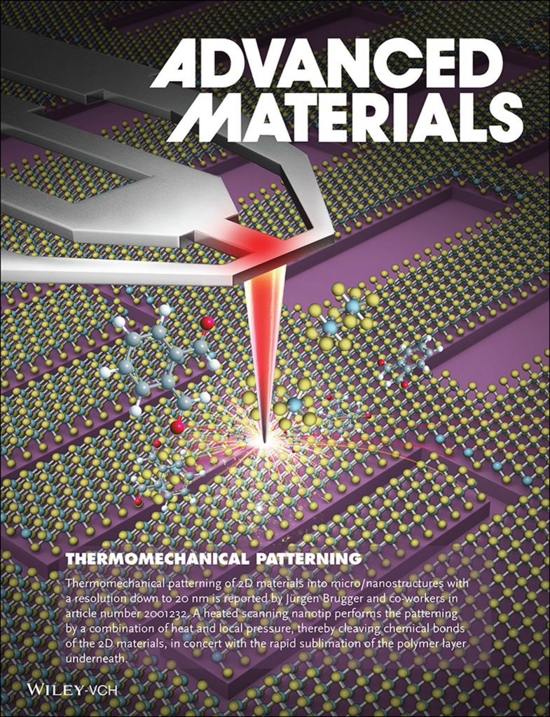
Advanced Materials. 2020. p. 2001232. DOI : 10.1002/adma.202001232.Additive micro-manufacturing of crack-free PDCs by two-photon polymerization of a single, low-shrinkage preceramic resin
Additive Manufacturing. 2020. p. 101343. DOI : 10.1016/j.addma.2020.101343.In Vitro Cytocompatibility Assessment of Ti-Modified, Silicon-oxycarbide-Based, Polymer-Derived, Ceramic-Implantable Electrodes under Pacing Conditions
ACS Applied Materials & Interfaces. 2020. Vol. 12, num. 15, p. 17244 – 17253. DOI : 10.1021/acsami.0c01465.Thermal scanning probe lithography-a review
Microsystems & Nanoengineering. 2020. Vol. 6, num. 1, p. 21. DOI : 10.1038/s41378-019-0124-8.Simply Structured Wearable Triboelectric Nanogenerator Based on a Hybrid Composition of Carbon Nanotubes and Polymer Layer
International Journal Of Precision Engineering And Manufacturing-Green Technology. 2020. Vol. 7, p. 683 – 698. DOI : 10.1007/s40684-020-00212-8.Na3V2(PO4)(3)-Supported Electrospun Carbon Nanofiber Nonwoven Fabric as Self-Standing Na-Ion Cell Cathode
Chemelectrochem. 2020. Vol. 7, num. 7, p. 1652 – 1659. DOI : 10.1002/celc.202000345.Thermal Scanning Probe Lithography for low dimensional materials
2020.Level-line moirés by superposition of cylindrical microlens gratings
Journal of the Optical Society of America. 2020. Vol. A37, num. 2, p. 209 – 218. DOI : 10.1364/JOSAA.37.000209.Cost-Effective Shape Memory Stamp for Laser Induced-Forward Transfer (LIFT)
2020.3D-Architecture Triboelectric Generator Using Deformable Liquid Metal
2020.Studying the interactions between electro-magnetic elds and biological tissue
2020.Electron Spin Resonance Magnetometers for Particle Accelerators
Lausanne, EPFL, 2020.3D Printed Micro-Scaffolds Loaded by Inkjet Printing With in-Precise Amount of Drug
2020. IEEE 15th International Conference on Nano/Micro Engineered and Molecular System (NEMS), ELECTR NETWORK, Sep 27-30, 2020. p. 426 – 429. DOI : 10.1109/NEMS50311.2020.9265525.Thermomechanical nanocutting of 2D materials using thermal scanning probe lithography
CMD2020GEFES, 2020 joint conference of the condensed matter divisions of EPS_CMD and RSEF-GEFES, Online, 31st August – 4th September, 2020.Transient Electronics for Smart Biodegradable Medical Implants
Lausanne, EPFL, 2020.3D-ARCHITECTURE TRIBOELECTRIC GENERATOR USING DEFORMABLE LIQUID METAL
2020
Design Concerns for In-body Antennas Based on Frequency Analysis of Fundamental Radiation Limitations
2020. 14th European Conference on Antennas and Propagation (EuCAP), Copenhagen, DENMARK, Mar 15-20, 2020. DOI : 10.23919/EuCAP48036.2020.9135679.Moiré effects produced by superpositions of micro-lens arrays
Lausanne, EPFL, 2020.Thermal Responsive Silk Composite Membrane for Magnetic Field Triggered Controllable Drug Delivery
Lausanne, EPFL, 2020.Miniaturized mr device comprising a cell culture micro-chamber and method for manufacturing such a device
ES2961924; JP7423084; EP3857247; EP3857247; US2022026379; JP2022502636; EP3857247; CN113167848; IL281764; WO2020065478.
2020.2019
1D moiré shapes by superposed layers of micro-lenses
Optics Express. 2019. Vol. 27, num. 26, p. 37419 – 37434. DOI : 10.1364/OE.27.037419.Printed silk-fibroin-based triboelectric nanogenerators for multi-functional wearable sensing
Nano Energy. 2019. Vol. 66, p. 104123. DOI : 10.1016/j.nanoen.2019.104123.Biodegradable Wireless Microheaters for Transient Biomedical Implants
NanoBioTech-Montreux, Montreux, Switzerland, November 20, 2019.Modeling of Total Ionizing Dose Degradation on 180-nm n-MOSFETs Using BSIM3
Ieee Transactions On Electron Devices. 2019. Vol. 66, num. 11, p. 4617 – 4622. DOI : 10.1109/TED.2019.2926931.Phase masks for electron microscopy fabricated by thermal scanning probe lithography
Micron. 2019. Vol. 127, p. 102753. DOI : 10.1016/j.micron.2019.102753.A 3D Microscaffold Cochlear Electrode Array for Steroid Elution
Advanced Healthcare Materials. 2019. p. 1900379. DOI : 10.1002/adhm.201900379.Harnessing Poisson Effect to Realize Tunable Tunneling Nanogap Electrodes on PDMS Substrates for Strain Sensing
2019. 20th International Conference on Solid-State Sensors, Actuators and Microsystems & Eurosensors XXXIII (TRANSDUCERS & EUROSENSORS XXXIII), Berlin, Germany, June 23-27, 2019. p. 2368 – 2371. DOI : 10.1109/TRANSDUCERS.2019.8808819.Liquid Assembly of Floating Nanomaterial Sheets for Transparent Electronics
Advanced Materials Technologies. 2019. p. 1900398. DOI : 10.1002/admt.201900398.Microwave inductive proximity sensors with sub-pm/Hz1/2 resolution
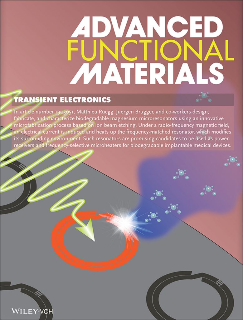
Sensors and Actuators A: Physical. 2019. Vol. 295, p. 259 – 265. DOI : 10.1016/j.sna.2019.05.041.Biodegradable Frequency‐Selective Magnesium Radio‐Frequency Microresonators for Transient Biomedical Implants
Advanced Functional Materials. 2019. Vol. 29, num. 39, p. 1903051. DOI : 10.1002/adfm.201903051.CMOS and 3D Printing for NMR Spectroscopy at the Single Embryo Scale
Chimia. 2019. Vol. 73, num. 7-8, p. 635 – 635. DOI : 10.2533/chimia.2019.635.Planar plasmonic antenna arrays resolve transient nanoscopic heterogeneities in biological membranes
2019. Joint 12th EBSA European Biophysics Congress / 10th IUPAP International Conference on Biological Physics (ICBP), Madrid, SPAIN, Jul 20-24, 2019. p. S107 – S107.Film Morphology Effect on VOC Sensor Performance Fabricated by Drop-On-Demand Inkjet-Printing
2019. 20th International Conference on Solid-State Sensors, Actuators and Microsystems and Eurosensors XXXIII (TRANSDUCERS and EUROSENSORS), Berlin, Germany, Jun 23-27, 2019. p. 1361 – 1364. DOI : 10.1109/TRANSDUCERS.2019.8808652.Optimization of the Bosch process for micro-mold fabrication
2019.Molding of Biodegradable Polymers for Drug Delivery Applications
2019.A Low-Power Microwave HEMT LC Oscillator Operating Down to 1.4 K
IEEE Transactions on Microwave Theory and Techniques. 2019. Vol. 67, num. 7, p. 2782 – 2792. DOI : 10.1109/TMTT.2019.2916552.Analog Control of Retainable Resistance Multistates in HfO2 Resistive-Switching Random Access Memories (ReRAMs)
Acs Applied Electronic Materials. 2019. Vol. 1, num. 6, p. 900 – 909. DOI : 10.1021/acsaelm.9b00094.Ferrimagnetic resonance field sensors for particle accelerators
Review Of Scientific Instruments. 2019. Vol. 90, num. 6, p. 065005. DOI : 10.1063/1.5097508.Self-Charging Energy Harvesting System for Wearables
Integration of SU8 lenses with 1310nm-wavelength wafer-fused vertical cavity surface emitting lasers (VCSELs)
LOPEC 2019.Integration of functionalization layers on lab-on-skin platform by inkjet printing
2019.Data logger for vacuum desiccator
2019.Biodegradable polymer for drug delivery applications
2019.Identifying suitable drugs for inkjet printing
2019.Inkjet printing of polymer composites for gas sensing applications
2019.Fabrication of 2D micro-lens arrays for moiré applications
2019.FEM Modelisation of membrane deformation
2019.Transient Electronics: Biodegradable Frequency‐Selective Magnesium Radio‐Frequency Microresonators for Transient Biomedical Implants (Adv. Funct. Mater. 39/2019)
Advanced Functional Materials. 2019. Vol. 29, num. 39, p. 1970270. DOI : 10.1002/adfm.201970270.Novel Wearable Triboelectric Generator based on a Hybrid Mix of Carbon Nanotube and Natural Polymer
MEMS, Seoul, Korea,Process optimization for thick SU-8 micro mold fabrication
2019.Multi-ReRAM synapses for artificial neural network training
2019. IEEE International Symposium on Circuits and Systems (IEEE ISCAS), Sapporo, JAPAN, May 26-29, 2019. DOI : 10.1109/ISCAS.2019.8702714.Electron Spin Resonance detectors from 400 MHz to 360 GHz
Lausanne, EPFL, 2019.A single-chip integrated transceiver for high field NMR magnetometry
Review Of Scientific Instruments. 2019. Vol. 90, num. 1, p. 015001. DOI : 10.1063/1.5066436.Wearable Triboelectric Generator based on a Hybrid Mix of Carbon Nanotube and Polymer Layers
2019. 18th International Conference on Micro and Nanotechnology for Power Generation and Energy Conversion Applications, Daytona Beach, FL, Dec 04-07, 2018. DOI : 10.1088/1742-6596/1407/1/012047.2018
Edge-contacted graphene with slope engineering by stencil lithography
2018.Fast turnaround fabrication of silicon point-contact quantum-dot transistors using combined thermal scanning probe lithography and laser writing
Nanotechnology. 2018. Vol. 29, num. 50, p. 505302. DOI : 10.1088/1361-6528/aae3df.Fabrication of Biodegradable Membrane
2018.Inkjet-printing polymer nanocomposite for detecting VOCs
2018. Eurosensors, Graz, September 9-12,2018.Unusually Long-Lived Photocharges in Helical Organic Semiconductor Nanostructures
Acs Nano. 2018. Vol. 12, num. 9, p. 9116 – 9125. DOI : 10.1021/acsnano.8b03165.A single chip electron spin resonance detector based on a single high electron mobility transistor
Journal of Magnetic Resonance. 2018. Vol. 294, p. 59 – 70. DOI : 10.1016/j.jmr.2018.07.002.Electronics for integrated oscillators phase noise characterization
2018.Electromechanical behavior of stencil-lithography-fabricated biocompatible gold contacts on PDMS substrates
2018.Combination of thermal scanning probe lithography and ion etching to fabricate 3D silicon nanopatterns with extremely smooth surface
Microelectronic Engineering. 2018. Vol. 193, p. 23 – 27. DOI : 10.1016/j.mee.2018.02.012.3D printed microchannels for sub-nL NMR spectroscopy
PLOS ONE. 2018. Vol. 13, num. 5, p. e0192780. DOI : 10.1371/journal.pone.0192780.Bioresorbable Frequency-Selective Magnesium Microresonators Fabricated by Ion Beam Etching
Microtechnologies in Medicine and Biology, Monterey, USA, 26-28 March 2018.Characterization of a Piezoelectric AlN Beam Array in Air and Fluid for an Artificial Basilar Membrane
Electronic Materials Letters. 2018. Vol. 14, num. 2, p. 101 – 111. DOI : 10.1007/s13391-018-0012-7.Growth of Large-Area 2D MoS2 Arrays at Pre-Defined Locations Using Stencil Mask Lithography
Journal of Nanoscience and Nanotechnology. 2018. Vol. 18, num. 3, p. 1824 – 1832. DOI : 10.1166/jnn.2018.14265.Nanostructured surface topographies have an effect on bactericidal activity
Journal of Nanobiotechnology. 2018. Vol. 16, num. 1, p. 20. DOI : 10.1186/s12951-018-0347-0.All-fiber hybrid piezoelectric-enhanced triboelectric nanogenerator for wearable gesture monitoring
Nano Energy. 2018. Vol. 48, p. 152 – 160. DOI : 10.1016/j.nanoen.2018.03.033.Characterization of Biodegradable Magnesium Resonators
2018.Integration of SU8 lenses with 1310nm-wavelength wafer-fused vertical cavity surface emitting lasers (VCSELs)
NANO.IL.2018.Study of Gd-induced shift of luminescence spectra of YGAG:Ce micropowders as a function of grain size
Journal of Luminescence. 2018. Vol. 196, p. 94 – 99. DOI : 10.1016/j.jlumin.2017.11.033.Synthesis and Investigation of Electrical Properties of Carbon Nanotube – Porous Matrix Composites near the Percolation Threshold
ORIENTAL JOURNAL OF CHEMISTRY. 2018. Vol. 34, num. 1, p. 24 – 29. DOI : 10.13005/ojc/340102.Nanoscale Lithography and Thermometry with Thermal Scanning Probes
Lausanne, EPFL, 2018.Fabrication and Characterization of Biodegradable, Thermal-Responsive Silk Composite Membrane
2018. The International Conference on Nano/Micro Engineered and Molecular Systems (NEMS), Singapore, 22-26, April 2018. p. 479 – 482. DOI : 10.1109/NEMS.2018.8556951.Optical Antenna-Based Fluorescence Correlation Spectroscopy to Probe the Nanoscale Dynamics of Biological Membranes
The Journal of Physical Chemistry Letters. 2018. num. 9, p. 110 – 119. DOI : 10.1021/acs.jpclett.7b02818.Unipolar Charging of Aerosol Particles in the Size Range of 75-500 nm by Needle-plate Corona Charger
ORIENTAL JOURNAL OF CHEMISTRY. 2018. Vol. 34, num. 1, p. 214 – 221. DOI : 10.13005/ojc/340124.The key impact of incorporated Al2O3 barrier layer on W-based ReRAM switching performance
2018. 15th International Conference on Synthesis, Modeling, Analysis and Simulation Methods and Applications to Circuit Design (SMACD) / 14th Conference on PhD Research in Microelectronics and Electronics (PRIME), Prague, CZECH REPUBLIC, Jul 02-05, 2018. p. 69 – 72. DOI : 10.1109/PRIME.2018.8430371.Tin Acetylacetonate as a Precursor for Producing Gas-Sensing SnO2 Thin Films
RUSSIAN JOURNAL OF INORGANIC CHEMISTRY. 2018. Vol. 63, num. 7, p. 851 – 860. DOI : 10.1134/S0036023618070197.PZE-transduced Suspended Microchannel Resonators for sensing applications
Lausanne, EPFL, 2018.All-in-one self-powered flexible microsystems based on triboelectric nanogenerators
Nano Energy. 2018. Vol. 47, p. 410 – 426. DOI : 10.1016/j.nanoen.2018.02.046.Applications of antibodies in microfluidics-based analytical systems: challenges and strategies for success
Journal of Micromechanics and Microengineering. 2018. Vol. 28, num. 6, p. 063001. DOI : 10.1088/1361-6439/aab225.Frame structure for thin-film piezoelectric-on-silicon resonator to greatly enhance quality factor and suppress spurious modes
SENSORS AND ACTUATORS A-PHYSICAL. 2018. Vol. 274, p. 101 – 108. DOI : 10.1016/j.sna.2018.03.012.2017
Micro-molding of biodegradable polymer for drug delivery applications
2017.Nanoparticle Manipulation with an AFM Probe
2017.Mode Evolution in Strongly Coupled Plasmonic Dolmens Fabricated by Templated Assembly
ACS Photonics. 2017. Vol. 4, num. 7, p. 1661 – 1668. DOI : 10.1021/acsphotonics.6b01026.Shape Memory Micro- and Nanowire Libraries for the High-Throughput Investigation of Scaling Effects
Acs Combinatorial Science. 2017. Vol. 19, num. 9, p. 574 – 584. DOI : 10.1021/acscombsci.7b00065.NMR spectroscopy of single sub-nL ova with inductive ultra-compact single-chip probes
Scientific Reports. 2017. Vol. 7, p. 44670. DOI : 10.1038/srep44670.Broadband IQ CMOS transceivers for compact and ultra-compact NMR probes
2017. 58th Experimental Nuclear Magnetic Resonance Conference, Asilomar Conference Grounds, Pacific Grove, California, March 26 – 31, 2017.Synthesis of superposition shape images by light interacting with layers of lenslets
CH713112; AU2016344585; EP3368332; US10899161; SE543208; RU2018119314; RU2018119314; PL426607; US10286716; CL2018001115; US2018311990; BR112018008671; GB2561731; CN108541238; EP3368332; MX2018005369; KR20180095802; AT519643; DE112016004552; GB201806957; SE1850632; AU2016344585; CA3002906; WO2017072566; US2017113481.
2017.Broadband single-chip transceivers for compact NMR probes
Lausanne, EPFL, 2017.High sensitivity field asymmetric ion mobility spectrometer
Review of Scientific Instruments. 2017. Vol. 88, num. 3, p. 035115 – 1. DOI : 10.1063/1.4978960.Flexible fabric-based wearable solid-state supercapacitor
2017. IEEE 12th International Conference on Nano/Micro Engineered and Molecular Systems (NEMS), Los Angeles, CA, USA, April 9-12, 2017. p. 169 – 172. DOI : 10.1109/NEMS.2017.8016998.Thermal Probe Nanopatterning Enables Nanoparticle Assembly on PDMS Substrates
43rd International Conference on Micro and NanoEngineering, Braga, Portugal, September 18-22, 2017.High-aspect ratio nanopatterning via combined thermal scanning probe lithography and dry etching
Microelectronic Engineering. 2017. Vol. 180, p. 20 – 24. DOI : 10.1016/j.mee.2017.04.006.The role of inkjet printing in tissue engineering
InPrint 2017, Munich, November 14-16, 2017.Penciling a triboelectric nanogenerator on paper for autonomous power MEMS applications
Nano Energy. 2017. Vol. 33, p. 393 – 401. DOI : 10.1016/j.nanoen.2017.01.053.Micro-moirés combining metallic patterns and micro-lenses
Micro and Nano Engineering (MNE), Braga, Portugal, September 18-22, 2017.Inkjet Printing of Functional Polymer Composites for Chemiresistive Gas Sensors
EDMI Day, EPFL, Lausanne, Switzerland,Control of the interaction strength of photonic molecules by nanometer precise 3D fabrication
Scientific Reports. 2017. Vol. 7, num. 1, p. 16502. DOI : 10.1038/s41598-017-16496-x.Single-chip electron spin resonance detectors operating at 50 GHz, 92 GHz, and 146 GHz
Journal of Magnetic Resonance. 2017. Vol. 278, p. 113 – 121. DOI : 10.1016/j.jmr.2017.03.013.Mode Coupling in Plasmonic Heterodimers Probed with Electron Energy Loss Spectroscopy
ACS Nano. 2017. Vol. 11, num. 4, p. 3485 – 3495. DOI : 10.1021/acsnano.6b08589.Planar Optical Nanoantennas Resolve Cholesterol-Dependent Nanoscale Heterogeneities in the Plasma Membrane of Living Cells
Nano Letters. 2017. Vol. 17, num. 10, p. 6295 – 6302. DOI : 10.1021/acs.nanolett.7b02973.In-Plane Plasmonic Antenna Arrays with Surface Nanogaps for Giant Fluorescence Enhancement
Nano Letters. 2017. Vol. 17, num. 3, p. 1703 – 1710. DOI : 10.1021/acs.nanolett.6b04978.Nanoscale topographical control of capillary assembly of nanoparticles
Nature Nanotechnology. 2017. Vol. 12, num. 1, p. 73 – 80. DOI : 10.1038/nnano.2016.179.Methods and microfabrication techniques for subnanoliter magnetic resonance spectroscopy
Lausanne, EPFL, 2017.Nanopatterning of a Stimuli-Responsive Fluorescent Supramolecular Polymer by Thermal Scanning Probe Lithography
ACS Applied Materials & Interfaces. 2017. Vol. 9, num. 47, p. 41454 – 41461. DOI : 10.1021/acsami.7b13672.Transient Nanoscopic Phase Separation in Biological Lipid Membranes Resolved by Planar Plasmonic Antennas
ACS Nano. 2017. Vol. 11, num. 7, p. 7241 – 7250. DOI : 10.1021/acsnano.7b03177.DOD Inkjet printing of functional polymers
CMI Day, EPFL, Lausanne, Switzerland,A transparent silk-fibroin-based triboelectric microgenerator for airflow energy harvesting
2017. IEEE 12th International Conference on Nano/Micro Engineered and Molecular Systems (NEMS), Los Angeles, CA, USA, April 9-12, 2017. p. 65 – 68. DOI : 10.1109/NEMS.2017.8016975.Printing wax to create scaffolds for tissue engineering applications
Swiss ePrint 2107, Basel, September 26-27, 2017.Self-assembly of micro/nanosystems across scales and interfaces
2017. 19th International Conference on Solid-State Sensors, Actuators and Microsystems (TRANSDUCERS 2017), Kaohsiung, Taiwan, June 18-22, 2017. p. 676 – 681. DOI : 10.1109/TRANSDUCERS.2017.7994139.Novel manufacturing methods for optical antennas : controlling light down to the single nanometer scale
Lausanne, EPFL, 2017.Nanoscale topography determines the capillary assembly of nanoparticles
13th Zsigmondy Colloquium of the German Colloidal Society, Saarbrücken, DE, April 5-7, 2017.Preceramic Polymers as Precursor for implantable MEMS Applications
11th NAMIS International Autumn School “Micro & nano systems engineering: from fundamentals to industrial applications”, Freiburg, Germany, October 2-6, 2017.Growth Of Organic Semiconductor Thin Films with Multi-Micron Domain Size and Fabrication of Organic Transistors Using a Stencil Nanosieve
ACS Applied Materials & Interfaces. 2017. Vol. 9, num. 28, p. 23314 – 23318. DOI : 10.1021/acsami.7b06584.Drop-on-Demand Inkjet Printing of Functional Composites
Swiss ePrint 2017 The Swiss Conference on Printed Electronics and Functional Materials, Basel, Switzerland, September 26-27, 2017.Thermal-responsive biodegradable composite membrane for drug delivery application
11th NAMIS international Autumn school “Micro & nano systems engineering: from fundamentals to industrial applications”, Freiburg, Germany, October 2-6, 2017.Silicon nanostructures for bright field full color prints
ACS Photonics. 2017. Vol. 4, num. 8, p. 1913 – 1919. DOI : 10.1021/acsphotonics.6b01021.Silk Fibroin as a Resist for Thermal Scanning Probe Lithography
43rd Micro and Nano Engineering Conference, Braga, Portugal, September 18-22, 2017.2016
Capillary assembly of nanoparticles Diamonds in antennas & durable Ag samples
2016.Evaluation of thermal scanning probe lithography patterns
2016.Fabrication d’antennes plasmoniques pour mesurer au TEM
2016.Spark discharge synthesis of semiconductor nanoparticles for thick-film metal oxide gas sensors
2016. 30th Eurosensors Conference, Eurosensors 2016, Budapest (HU), 4-7.9.2016. p. 1036 – 1039. DOI : 10.1016/j.proeng.2016.11.334.Rapid carbon nanotubes suspension in organic solvents using organosilicon polymers
Journal of Colloid and Interface Science. 2016. Vol. 470, num. 15, p. 123 – 131. DOI : 10.1016/j.jcis.2016.02.050.NMR spectroscopy of subnanoliter ova with ultra-compact inductive probes
2016. EUROMAR 2016, Aarhus, Denmark, July 3-7, 2016.Plasmonic photoconductance in free-standing monolayered gold nanoparticle membranes
2016. 11th IEEE Nanotechnology Materials and Devices Conference (NMDC), Toulouse, FRANCE, OCT 09-12, 2016. DOI : 10.1109/NMDC.2016.7777131.A low-power high-sensitivity single-chip receiver for NMR microscopy
Journal of Magnetic Resonance. 2016. Vol. 266, p. 41 – 50. DOI : 10.1016/j.jmr.2016.03.004.Electrical Investigation of Porous Silicon/p-Si Heterojunction Prepared by Electrochemical Etching
Ecs Journal Of Solid State Science And Technology. 2016. Vol. 5, num. 4, p. P3172 – P3175. DOI : 10.1149/2.0241604jss.Penciling A Triboelectric Power Source On Paper
2016. 29th IEEE International Conference on Micro Electro Mechanical Systems (MEMS), Shanghai, PEOPLES R CHINA, JAN 24-28, 2016. p. 1169 – 1172. DOI : 10.1109/MEMSYS.2016.7421844.High sensitivity field asymmetric ion mobility spectrometer
Lausanne, EPFL, 2016.Thermal scanning probe lithography on a glassy supramolecular film creates a combination of topogrpahy and fluroescent nanostructures
42nd Micro and Nano Engineering Conference, Vienna, Austria, September 20-23, 2016.Arrays of Pentacene Single Crystals by Stencil Evaporation
Crystal Growth & Design. 2016. Vol. 16, p. 4694−4700. DOI : 10.1021/acs.cgd.6b00765.Harnessing the damping properties of materials for high-speed atomic force microscopy
Nature Nanotechnology. 2016. Vol. 11, p. 147 – 151. DOI : 10.1038/NNANO.2015.254.Electro-mechanical sensing in freestanding monolayered gold nanoparticle membranes
Nanoscale. 2016. Vol. 8, num. 22, p. 11363 – 11370. DOI : 10.1039/C6NR02004F.Bi-directional AC electrothermal micropump for on-chip biological applications
ELECTROPHORESIS. 2016. Vol. 37, num. 5-6, p. 719 – 726. DOI : 10.1002/elps.201500404.3D nanostructures fabricated by advanced stencil lithography
Nanoscale. 2016. Vol. 9, p. 4945 – 4950. DOI : 10.1039/C5NR08444J.Exploring Nanoscale Electrical Properties of CuO-Graphene Based Hybrid Interfaced Memory Device by Conductive Atomic Force Microscopy
Journal of Nanoscience and Nanotechnology. 2016. Vol. 16, num. 4, p. 4044 – 4051. DOI : 10.1166/jnn.2016.10713.Antibacterial Au nanostructured surfaces
Nanoscale. 2016. Vol. 8, num. 5, p. 2620 – 2625. DOI : 10.1039/C5NR06157A.Scanning thermal probe microscope method for the determination of thermal diffusivity of nanocomposite thin films
Review Of Scientific Instruments. 2016. Vol. 87, num. 8, p. 084903. DOI : 10.1063/1.4960332.A silk-fibroin-based transparent triboelectric generator suitable for autonomous sensor network
Nano Energy. 2016. Vol. 20, p. 37 – 47. DOI : 10.1016/j.nanoen.2015.11.036.Highly efficient and gentle trapping of single cells in large microfluidic arrays for time-lapse experiments
Biomicrofluidics – Fundamentals, Perspectives & Applications. 2016. Vol. 10, num. 1, p. 014120. DOI : 10.1063/1.4942457.Impedance spectroscopy study of carbon nanotube–glass microfiber composites
Oriental Journal of Chemistry. 2016. Vol. 32, num. 6, p. 2857 – 2861. DOI : 10.13005/ojc/320603.Plasmonic photo-current in freestanding monolayered gold nanoparticle membranes
Nanoscale. 2016. Vol. 8, num. 36, p. 16162 – 16167. DOI : 10.1039/c6nr05091c.2015
AFM Tips for Measurements and Manipulation of Fluid Interfaces
2015.DESIGN, FABRICATION, AND CHARACTERIZATION OF AFM TIPS FOR TENSIONS MEASUREMENT AND MANIPULATION OF FLUID INTERFACES
2015.Fabrication and Replication of Microlens Arrays for Confocal Microscopy
2015.FUTURE POWER POWERING FUTURE: HIGH-PERFORMANCE TRIBOELECTRIC NANOGENERATOR FOR WEARABLE ELECTRONICS
2015. 2015 JSME-IIP/ASME-ISPS Joint Conference on Micromechatronics for Information and Precision Equipment (MIPE 2015), Kobe, Japan, June 14-17, 2015.Large-Scale Arrays of Bowtie Nanoaperture Antennas for Nanoscale Dynamics in Living Cell Membranes
Nano Letters. 2015. Vol. 15, num. 6, p. 4176 – 4182. DOI : 10.1021/acs.nanolett.5b01335.CNT and PDCs: A fruitful association? Study of a polycarbosilane–MWCNT composite
Journal of the European Ceramic Society. 2015. Vol. 35, num. 8, p. 2215 – 2224. DOI : 10.1016/j.jeurceramsoc.2015.02.016.Organic-inorganic-hybrid-polymer microlens arrays with tailored optical characteristics and multi-focal properties
Optics Express. 2015. Vol. 23, num. 19, p. 25365 – 25376. DOI : 10.1364/OE.23.025365.On the micrometre precise mould filling of liquid polymer derived ceramic precursor for 300-µm-thick high aspect ratio ceramic MEMS
Ceramics International. 2015. Vol. 41, num. 1, p. 623 – 629. DOI : 10.1016/j.ceramint.2014.08.112.Transflective holographic film for head worn display
US2015362734; WO2014115095; WO2014115095.
2015.A broadband single-chip transceiver for multi-nuclear NMR probes
Review Of Scientific Instruments. 2015. Vol. 86, num. 4, p. 044703. DOI : 10.1063/1.4916206.Effects of the Discharge Parameters on the Efficiency and Stability of Ambient Metastable-Induced Desorption Ionization
Plasma Science & Technology. 2015. Vol. 17, num. 12, p. 1048 – 1052. DOI : 10.1088/1009-0630/17/12/12.Cytotoxicity evaluation of polymer-derived ceramics for pacemaker electrode applications
Journal of Biomedical Materials Research Part A. 2015. Vol. 103, num. 11, p. 3625 – 3632. DOI : 10.1002/jbm.a.35477.Electrical Property of Platinum Micro Heater for Thermal Analysis of Microfluidic Device
IEEJ Transactions on Sensors and Micromachines. 2015. Vol. 135, num. 8, p. 338 – 342. DOI : 10.1541/ieejsmas.135.338.Cryogenic single chip electron spin resonance detectors
Lausanne, EPFL, 2015.Impedance sensing of DNA immobilization and hybridization by microfabricated alumina nanopore membranes
Sensors and Actuators B: Chemical. 2015. Vol. 216, p. 105 – 112. DOI : 10.1016/j.snb.2015.03.094.Composite hydrogel-loaded alumina membranes for nanofluidic molecular filtration
Journal of Membrane Science. 2015. Vol. 477, num. 1, p. 151 – 156. DOI : 10.1016/j.memsci.2014.12.023.Resistless nanofabrication by stencil lithography: A review
Microelectronic Engineering. 2015. Vol. 132, p. 236 – 254. DOI : 10.1016/j.mee.2014.08.003.Fabrication of complex oxide microstructures by combinatorial chemical beam vapour deposition through stencil masks
Thin Solid Films. 2015. Vol. 586, p. 64 – 69. DOI : 10.1016/j.tsf.2015.04.021.Investigation of liquid pinning on surface nanoscale topography
2015.Foil-to-Foil System Integration Through Capillary Self-Alignment Directed by Laser Patterning
Journal of Microelectromechanical Systems. 2015. Vol. 24, num. 1, p. 126 – 133. DOI : 10.1109/JMEMS.2014.2321013.Development of Implantable Electrodes Based on Polymer Derived Ceramics
Lausanne, EPFL, 2015.2014
Nanoparticle assembly : scalable process development from nanoscale molding to hardware/software implementation
2014.Microfluidic cell trapping structures for single-cell experiments
2014.Capillary particle assembly (CAPA) for plasmonic devices
2014.Frequency jumps in single chip microwave LC oscillators
Applied Physics Letters. 2014. Vol. 105, num. 24, p. 242102. DOI : 10.1063/1.4904417.Direct imprinting of organic-inorganic hybrid materials into high aspect ratio sub-100 nm structures
Microsystem Technologies-Micro-And Nanosystems-Information Storage And Processing Systems. 2014. Vol. 20, num. 10-11, p. 1961 – 1966. DOI : 10.1007/s00542-013-2016-4.High-yield and high-precision nanoparticle assembly: towards complex plasmonic antennas
40th International Conference on Micro and Nano Engineering (MNE 2014), Lausanne, CH, September 22-26, 2014.Influence of carbon enrichment on electrical conductivity and processing of polycarbosilane derived ceramic for MEMS applications
Journal of the European Ceramic Society. 2014. Vol. 34, num. 15, p. 3559 – 3570. DOI : 10.1016/j.jeurceramsoc.2014.06.002.UV-Imprinting and Inkjet Printing – A Technology Synergy for Microlens Manufacturing
2014. 13th International Conference on Nanoimprint and Nanoprint Technology (NNT 2014), Kyoto, Japan, October 22-24.UV-Imprint Resists Generated from Polymerizable Ionic Liquids and Titania Nanoparticles
The Journal of Physical Chemistry C. 2014. Vol. 118, p. 16743−16748. DOI : 10.1021/jp412722y.Polymeric variable optical attenuators based on magnetic sensitive stimuli materials
Journal Of Micromechanics And Microengineering. 2014. Vol. 24, num. 12, p. 125008. DOI : 10.1088/0960-1317/24/12/125008.Microdrop generation and deposition of ionic liquids
Journal Of Materials Research. 2014. Vol. 29, num. 17, p. 2100 – 2107. DOI : 10.1557/jmr.2014.162.Three Dimensional Microstructures for Cell Culture with Engineered Stiffness and Geometry
Lausanne, EPFL, 2014.Cryogenic single-chip electron spin resonance detector
Journal of Magnetic Resonance. 2014. Vol. 247, p. 96 – 103. DOI : 10.1016/j.jmr.2014.08.013.Inkjet Printing of High Aspect Ratio Superparamagnetic SU-8 Microstructures with Preferential Magnetic Directions
Micromachines. 2014. Vol. 5, p. 583 – 593. DOI : 10.3390/mi5030583.Automated Real-Time Control of Fluidic Self-Assembly of Microparticles
2014. 2014 IEEE International Conference on Robotics and Automation (ICRA 2014), Hong Kong (China), May 31 – June 7, 2014. p. 5860 – 5865. DOI : 10.1109/ICRA.2014.6907721.Thermal analysis, design and fabrication of microfluidic device with local temperature controls
2014. The 7th Asia-Pacific Conference on Transducers and Micro/Nano Technologies, Daegu, Korea, June 29- July 2, 2014. DOI : 10.11188/seisankenkyu.66.281.Liquid-Filled Sealed Mems Capsules Fabricated By Fluidic Self-Assembly
2014. IEEE International Conference on Micro Electro Mechanical Systems (MEMS 2014), San Francisco (USA), January 26-30, 2014. p. 56 – 59. DOI : 10.1109/MEMSYS.2014.6765572.PDMS-based, magnetically actuated variable optical attenuators obtained by soft lithography and inkjet printing technologies
Sensors And Actuators A-Physical. 2014. Vol. 215, p. 30 – 35. DOI : 10.1016/j.sna.2014.01.021.UV-patternable polymers with selective spectral response (vol 98, pg 234, 2013)
Microelectronic Engineering. 2014. Vol. 115, p. 1 – 1. DOI : 10.1016/j.mee.2013.10.019.Fabrication of HepG2 Cell Laden Collagen Microspheres using Inkjet Printing
Journal of the Korean Society for Precision Engineering. 2014. Vol. 31, num. 8, p. 743 – 747. DOI : 10.7736/KSPE.2014.31.8.743.LOCALIZED EXPRESSION OF HEAT SHOCK PROTEIN IN CELL POPULATION BY MICRO HEATER DEVICE
MICROTAS 2014, TX 78205, USA, October 26-30, 2014.Actuated MEMS and NEMS for cell force spectroscopy and gas sensing applications
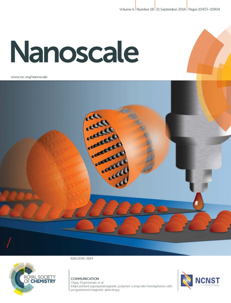
Lausanne, EPFL, 2014.Inkjet printed superparamagnetic polymer composite hemispheres with programmed magnetic anisotropy
Nanoscale. 2014. Vol. 6, p. 10495 – 10499. DOI : 10.1039/C3NR06442E.Curved Holographic Combiner for Color Head Worn Display
Journal Of Display Technology. 2014. Vol. 10, num. 6, p. 444 – 449. DOI : 10.1109/Jdt.2013.2277933.Single-Cell 3D Bio-Mems Environment With Engineered Geometry And Physiologically Relevant Stiffnesses
2014. 27th IEEE International Conference on Micro Electro Mechanical Systems (MEMS), San Francisco, CA, JAN 26-30, 2014. p. 177 – 180. DOI : 10.1109/MEMSYS.2014.6765603.Grazing angle X-ray fluorescence from periodic structures on silicon and silica surfaces
2014. 15th International Conference on Total Reflection X-ray Fluorescence Analysis and Related Methods / 49th Annual Conference on X-ray Chemical Analysis (TXRF), Osaka, JAPAN, SEP 23-27, 2013. p. 65 – 75. DOI : 10.1016/j.sab.2014.03.015.Three-dimensional polymeric microtiles for optically-tracked fluidic self-assembly
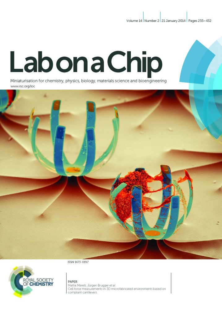
Microelectronic Engineering. 2014. Vol. 124, p. 1 – 7. DOI : 10.1016/j.mee.2014.04.017.Cell force measurements in 3D microfabricated environments based on compliant cantilevers
Lab on a Chip. 2014. Vol. 14, num. 2, p. 286 – 293. DOI : 10.1039/c3lc51021b.Shift Dynamics of Capillary Self-Alignment
2014. International Precision Assembly Seminar (IPAS 2014), Chamonix, FR, February 16-18, 2014. p. 61 – 68. DOI : 10.1007/978-3-662-45586-9_9.2013
Fabrication of transparent moiré based optically variable devices
2013.Study, design and testing of cryogenic electronics for EPR spectroscopy
2013.Heated mask
WO2012164546; WO2012164546.
2013.Resistless Fabrication of Nanoimprint Lithography (NIL) Stamps Using Nano-Stencil Lithography
Micromachines. 2013. Vol. 4, p. 370 – 377. DOI : 10.3390/mi4040370.Fluid-mediated self-assembly of MEMS micro-capsules for liquid encapsulation and release
Lausanne, EPFL, 2013.Integrated long-range thermal bimorph actuators for parallelizable bio-AFM applications
IEEE Sensors Journal. 2013. Vol. 13, num. 8, p. 2849 – 2856. DOI : 10.1109/JSEN.2013.2261293.Design iterations on Lego R – like MEMS bricks
2013.Three-dimensional SU-8 microtiles for fluidic self-assembly
2013. 39th International Conference on Micro and Nano Engineering (MNE 2013), London, 16-19 September 2013.Al2O3/W hetero-structured nanopore membranes: From native to tunable nanofluidic diodes
2013. 8th IEEE International Conference on Nano/Micro Engineered and Molecular Systems (NEMS), Suzhou, China, April 7-10, 2013. p. 998 – 1001. DOI : 10.1109/NEMS.2013.6559890.Polymeric hemispherical pico-liter micro cups fabricated by inkjet printing
2013. 2013 8th IEEE International Conference on Nano/Micro Engineered and Molecular Systems (NEMS), Suzhou, China, 7-10 04 2013. p. 1119 – 1122. DOI : 10.1109/NEMS.2013.6559918.Acousto-fluidic system assisting in-liquid self-assembly of microcomponents
Journal of Micromechanics and Microengineering. 2013. Vol. 23, num. 12, p. 125026. DOI : 10.1088/0960-1317/23/12/125026.Dynamics of capillary self-alignment for mesoscopic foil devices
Applied Physics Letters. 2013. Vol. 102, p. 144101. DOI : 10.1063/1.4801088.Simple and easily controllable parabolic-shaped microlenses printed on polymeric mesas
Journal Of Materials Chemistry C. 2013. Vol. 1, num. 11, p. 2152 – 2157. DOI : 10.1039/c3tc00632h.Stencil-Nanopatterned Back Reflectors for Thin-Film Amorphous Silicon n-i-p Solar Cells
Ieee Journal Of Photovoltaics. 2013. Vol. 3, num. 1, p. 22 – 26. DOI : 10.1109/Jphotov.2012.2213583.Application of stencil masks for ion beam lithographic patterning
Nuclear Instruments and Methods in Physics Research Section B: Beam Interactions with Materials and Atoms. 2013. Vol. 306, p. 292 – 295. DOI : 10.1016/j.nimb.2012.12.064.Field effect modulated nanofluidic diode membrane based on Al2O3/W heterogeneous nanopore arrays
Applied Physics Letters. 2013. Vol. 102, num. 21, p. 213108.1 – 4. DOI : 10.1063/1.4807781.Lateral capillary forces
Surface tension in microsystems; Springer, 2013. p. 45 – 69.In-liquid MEMS assembly by optical trapping
2013. 2013 IEEE 26th International Conference on Micro Electro Mechanical Systems (MEMS), Taipei, Taiwan, 20-24 01 2013. p. 78 – 81. DOI : 10.1109/MEMSYS.2013.6474181.Light spectral filtering based on spatial adiabatic passage
Light-Science & Applications. 2013. Vol. 2, p. e90. DOI : 10.1038/lsa.2013.46.Surface tension-driven self-assembly
Surface tension in microsystems; Berlin Heidelberg: Springer, 2013. p. 227 – 253.Preface: Special Issue: Euromat 2011-European Congress and Exhibition on Advanced Materials and Processes: Symposium A53 MEMS/NEMS for Sensorial and Actorial Materials
Journal Of Intelligent Material Systems And Structures. 2013. Vol. 24, num. 18, p. 2171 – 2171. DOI : 10.1177/1045389X13507157.Cell shape-dependent early responses of fibroblasts to cyclic strain
Biochimica et Biophysica Acta (BBA) – Molecular Cell Research. 2013. Vol. 1833, num. 12, p. 3415 – 3425. DOI : 10.1016/j.bbamcr.2013.10.012.Reconfigurable MEMS modules for 2D (self-)assembly
2013.Fluid-mediated parallel self-assembly of polymeric micro-capsules for liquid encapsulation and release
Soft Matter. 2013. Vol. 9, p. 9931 – 9938. DOI : 10.1039/c3sm51923f.Special Issue on Selected Papers From the 11th IEEE Sensors Conference 2012
Ieee Sensors Journal. 2013. Vol. 13, num. 8, p. 2809 – 2809. DOI : 10.1109/Jsen.2013.2268687.Room temperature strong coupling between a microwave oscillator and an ensemble of electron spins
Journal of Magnetic Resonance. 2013. Vol. 231, p. 133 – 140. DOI : 10.1016/j.jmr.2013.04.004.High aspect ratio etching of nanopores in PECVD SiC through AAO mask
2013. 8th Annual IEEE International Conference on Nano/Micro Engineered and Molecular Systems, Suzhou, China, April 7-10, 2013. p. 986 – 989. DOI : 10.1109/NEMS.2013.6559887.Structural and optical properties of the Cu2ZnSnSe4 thin films grown by nano-ink coating and selenization
Journal Of Materials Science-Materials In Electronics. 2013. Vol. 24, num. 2, p. 529 – 535. DOI : 10.1007/s10854-012-0970-8.Large-Area Gold/Parylene Plasmonic Nanostructures Fabricated by Direct Nanocutting
Advanced Optical Materials. 2013. Vol. 1, num. 1, p. 50 – 54. DOI : 10.1002/adom.201200017.High-resolution 1D moirés as counterfeit security features
Light: Science & Applications. 2013. Vol. 2, num. 7, p. e86. DOI : 10.1038/lsa.2013.42.Individually actuated cantilever arrays for cell force spectroscopy
Nano-Tera annual plenary meeting, Bern, Switzerland, May 30-31, 2013.Hot Stencils : A New Path for Resistless Nanopatterning
Lausanne, EPFL, 2013.Inkjet-printed SU-8 Hemispherical Microcapsules and Silicon chip Embedding
Micro & Nano Letters. 2013. Vol. 8, num. 10, p. 633 – 636. DOI : 10.1049/mnl.2013.0241.Simulation of Electrical Discharge Initiated by a Nanometer-Sized Probe in Atmospheric Conditions
Plasma Science & Technology. 2013. Vol. 15, num. 9, p. 845. DOI : 10.1088/1009-0630/15/9/02.Single Superparamagnetic Bead Detection and Direct Tracing of Bead Position Using Novel Nanocomposite Nano-Hall Sensors
Ieee Transactions On Nanotechnology. 2013. Vol. 12, num. 5, p. 668 – 673. DOI : 10.1109/Tnano.2013.2266733.2012
High Aspect Ratio Microstructures
2012.Miniaturized Ag/AgCl electrodes made by inkjet printing
2012.Heated membranes for stencil lithography application
2012.Nano-channel fabrication by electrostatic inkjet printing for the study of proton conductivity
2012.Fabrication & Characterization of Thermally Actuated MEMS
2012.Atomic Force Measurements of Hydrophobic Interactions
2012.Simulation of Optical Nanostructures
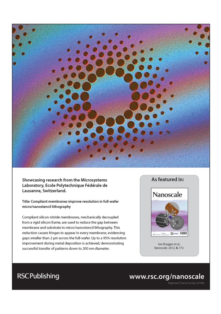
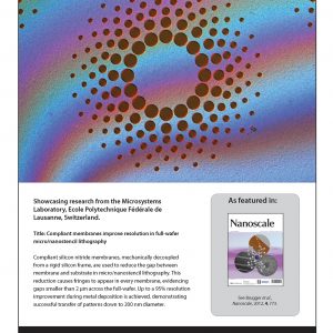
2012.Compliant membranes improve resolution in full-wafer micro/nanostencil lithography
Nanoscale. 2012. Vol. 4, p. 773 – 778. DOI : 10.1039/c2nr11609j.Integrated long-range thermal bimorph actuators for parallelizable bio-AFM applications
2012. 11th IEEE Sensors Conference, Taipei, Taiwan, October 28-31, 2012. p. 789 – 792. DOI : 10.1109/ICSENS.2012.6411507.Nanocomposites based on highly luminescent nanocrystals and semiconducting conjugated polymer for inkjet printing
Nanotechnology. 2012. Vol. 23, num. 7, p. 075701. DOI : 10.1088/0957-4484/23/7/075701.Biomimetic soft lithography on curved nanostructured surfaces
2012. September 19-23, Berlin, Germany, p. 269 – 271. DOI : 10.1016/j.mee.2012.03.013.Directly fabricated multi-scale microlens arrays on a hydrophobic flat surface by a simple ink-jet printing technique
Journal of Materials Chemistry. 2012. Vol. 22, num. 7, p. 3053 – 3058. DOI : 10.1039/c2jm15576a.Organic half-wave rectifier fabricated by stencil lithography on flexible substrate
Microelectronic Engineering. 2012. Vol. 100, p. 47 – 50. DOI : 10.1016/j.mee.2012.07.110.Highly inorganic titania based sol–gel as directly patternable resist for micro- and nano- structured surfaces
Microelectronic Engineering. 2012. Vol. 98, p. 176 – 179. DOI : 10.1016/j.mee.2012.07.043.UV-patternable polymers with selective spectral response
Microelectronic Engineering. 2012. Vol. 98, p. 234 – 237. DOI : 10.1016/j.mee.2012.07.013.Stencil-nanopatterned back reflectors for thin-film amorphous silicon n-i-p solar cells
2012. 38th IEEE Photovoltaic Specialists Conference (PVSC). p. 694 – 696. DOI : 10.1109/PVSC.2012.6317704.Vertically-stacked gate-all-around polysilicon nanowire FETs with sub-μm gates patterned by nanostencil lithography
Microelectronic Engineering. 2012. Vol. 98, p. 355 – 358. DOI : 10.1016/j.mee.2012.07.048.Fabrication of epoxy spherical microstructures by controlled drop-on-demand inkjet printing
Journal of Micromechanics and Microengineering. 2012. Vol. 22, num. 7, p. 074012. DOI : 10.1088/0960-1317/22/7/074012.3D hybrid microcomponents self-assembled in liquid
2012. 38th International Conference on Micro and Nano Engineering, Toulouse, France, September 16-20, 2012.All-stencil transistor fabrication on 3D silicon substrates
Journal of Micromechanics and Microengineering. 2012. Vol. 22, num. 9, p. 095022. DOI : 10.1088/0960-1317/22/9/095022.Conductivity of SU-8 Thin Films through Atomic Force Microscopy Nano-Patterning
Advanced Functional Materials. 2012. Vol. 22, num. 7, p. 1482 – 1488. DOI : 10.1002/adfm.201102789.Inkjet printing for MEMS
Inkjet-based Micromanufacturing; Germany: Wiley-VCH, 2012. p. 331 – 346.Thermal control extends heated stencil’s life-time
2012. The 56th International Conference on Electron, Ion, Photon Beam Technology and Nanofabrication, Waikoloa, Hawaii, USA, May 29 – June 1, 2012.Design, Modeling and Optimization of Stochastic Reactive Distributed Robotic Systems
Lausanne, EPFL, 2012.Capteur pour la detection d’hydrogene et procede de fabrication d’un tel capteur
FR2921159; FR2921159.
2012.K-band single-chip electron spin resonance detector
Journal of Magnetic Resonance. 2012. Vol. 217, p. 19 – 26. DOI : 10.1016/j.jmr.2012.02.003.Ultra-low power hydrogen sensing based on a palladium-coated nanomechanical beam resonator
Nanoscale. 2012. Vol. 4, num. 16, p. 5059 – 5064. DOI : 10.1039/C2NR30639E.CAFM investigations of filamentary conduction in Cu2O ReRAM devices fabricated using stencil lithography technique
Nanotechnology. 2012. Vol. 23, num. 49, p. 495707. DOI : 10.1088/0957-4484/23/49/495707.Active Integrated Tracking Detectors for MRI-Guided Interventions
Biomedical Engineering-Biomedizinische Technik. 2012. Vol. 57, p. 907. DOI : 10.1515/bmt-2012-4407.OPTIMIZATION OF THE PHOTOPOLYMERIZATION OF A POLYMER DERIVED CERAMIC
2012. 38th International Micro & Nano Engineering Conference, Toulouse, France, September 16-20, 2012.Hydrodynamic Trap for Directed Self-Assembly of MEMS
2012. The 7th Annual IEEE International Conference on Nano/Micro Engineered and Molecular Systems, Kyoto, JAPAN, March 5 – 8, 2012.High-Resolution Resistless Nanopatterning on Polymer and Flexible Substrates for Plasmonic Biosensing Using Stencil Masks
ACS Nano. 2012. Vol. 6, num. 6, p. 5474 – 5481. DOI : 10.1021/nn301358n.Sub micrometer ceramic structures fabricated by molding a polymer-derived ceramic
2012. Micro- and Nano-Engineering (MNE) 2011, Berlin, Germany, September 19-23, 2011. p. 272 – 275. DOI : 10.1016/j.mee.2012.04.024.In-situ actuated gap reduction and clogging-free apertures for quasi-dynamic stencil lithography
2012. The 7th Annual IEEE International Conference on Nano/Micro Engineered and Molecular Systems, Kyoto, JAPAN, March 5 – 8, 2012.Failure Modes in Capillary Self-Assembly
Micromanipulation for micro-nano systems, Femto-ST, Besancon, FR, April 11, 2012.The Solution of Nonlinear Function of Ion Mobility Based on FAIMS Spectrum Peak Position
Spectroscopy And Spectral Analysis. 2012. Vol. 32, num. 8, p. 2050 – 2055. DOI : 10.3964/j.issn.1000-0593(2012)08-2050-06.Facile fabrication of nanofluidic diode membranes using anodic aluminium oxide
Nanoscale. 2012. Vol. 4, num. 18, p. 5718 – 5723. DOI : 10.1039/c2nr31243c.Heterogeneous material micro-transfer by ink-jet print assisted mould filling
Microelectronic Engineering. 2012. Vol. 98, p. 619 – 622. DOI : 10.1016/j.mee.2012.04.025.Capillary Self-Alignment of Mesoscopic Foil Components for Sensor-Systems-in-Foil
Journal of Micromechanics and Microengineering. 2012. Vol. 22, p. 115022. DOI : 10.1088/0960-1317/22/11/115022.Modélisation du comportement non-linéaire des spins électroniques couplés à un oscillateur électrique
2012.Microdrop Printing of Hydrogel Bioinks into 3D Tissue-Like Geometries
Advanced Materials. 2012. Vol. 24, num. 3, p. 391 – 396. DOI : 10.1002/adma.201102800.Effects of tensile stress on electrical parameters of thin film conductive wires fabricated on a flexible substrate using stencil lithography
Microelectronic Engineering. 2012. Vol. 98, p. 230 – 233. DOI : 10.1016/j.mee.2012.07.016.Highly ordered palladium nanodot patterns for full concentration range hydrogen sensing
Nanoscale. 2012. Vol. 4, p. 1964 – 1967. DOI : 10.1039/C2NR11983H.Integrated active tracking detector for MRI-guided interventions
Magnetic Resonance In Medicine. 2012. Vol. 67, p. 290 – 296. DOI : 10.1002/mrm.23112.Mechanical and tribological properties of polymer-derived Si/C/N sub-millimetre thick miniaturized components fabricated by direct casting
Journal of the European Ceramic Society. 2012. Vol. 32, num. 8, p. 1759 – 1767. DOI : 10.1016/j.jeurceramsoc.2012.01.007.Phenyl-bridged polysilsesquioxane positive and negative resist for electron beam lithography
Nanotechnology. 2012. Vol. 23, p. 325302. DOI : 10.1088/0957-4484/23/32/325302.Streched organic transistors maintain mobility on flexible substrates
Microelectronic Engineering. 2012. Vol. 98, p. 508 – 511. DOI : 10.1016/j.mee.2012.07.080.2011
Inkjet printing of SU-8 based superparamagnetic composite
2011.Coating high aspect-ratio channels of multi-aperture vision sensor using Micromoulding in Capillaries (MIMIC)
2011.3D cell-cages for cell micro-environment engineering
2011.Micro-beams with tunable stiffness and curvature for mechano-sensitive cell culture substrates
37th International Conference on Micro and Nano Engineering, Berlin, Germany, September 19-23, 2011.High Throughput Nanofabrication of Silicon Nanowire and Carbon Nanotube Tips on AFM Probes by Stencil-Deposited Catalysts
Nano Letters. 2011. Vol. 11, num. 4, p. 1568 – 1574. DOI : 10.1021/nl104384b.Robust PECVD SiC membrane made for stencil lithography
2011. 36th International Conference on Micro & Nano Engineering (MNE), Genoa, Italy, September 19-22, 2010. p. 2790 – 2793. DOI : 10.1016/j.mee.2010.11.056.Nanostructured high refractive index titanium oxide films
E-MRS ICAM IUMRS 2011 Spring Meeting, France, Nice, May 9-13, 2011.3D Patterning of Hydrogels and Cells by Multi-Component Inkjet Printing
Swiss-eprint, Basel, Switzerland, December, 1-2, 2011.Integrated MEMS actuation for force spectroscopy in liquid
Nano-Tera Annual Plenary Meeting, Bern, CH, May 12-13, 2011.Microlenses with defined contour shapes
Optics Express. 2011. Vol. 19, num. 19, p. 18665. DOI : 10.1364/OE.19.018665.Advances in Nanostenciling: resistless nanopatterning enables new applications
Swiss NanoConvention, Baden, Switzerland, May 18-19, 2011.Vertically-Aligned Carbon Nanotubes for Supercapacitor and the Effect of Surface Functionalization to its Performance
Reliable and Improved Nanoscale Stencil Lithography by Membrane Stabilization, Blurring and Clogging Corrections
IEEE Transactions on Nanotechnology. 2011. Vol. 10, num. 2, p. 352 – 357. DOI : 10.1109/TNANO.2010.2042724.GOLD MEMBRANES WITH LARGE ARRAYS OF SUB-µm HOLES FABRICATED BY WAFER-SCALE NANOSPHERE LITHOGRAPHY
2011. The 16th International Conference on Solid-State Sensors, Actuators and Microsystems, Beijing, China, June 5-9, 2011.100 mm dynamic stencils pattern sub-micrometre structures
Nanoscale. 2011. Vol. 3, num. 7, p. 2739. DOI : 10.1039/c1nr10083a.Photon energy dependence of the light pressure exerted onto a thin silicon slab
Physical Review B – Condensed Matter and Materials Physics. 2011. Vol. 83, num. 16, p. 165321. DOI : 10.1103/PhysRevB.83.165321.Containers assembled in fluid and corresponding production
US2012145572; WO2010122499; WO2010122499.
2011.Hydrophobic Forces in Liquid Selfassembly
Nano-Tera Annual Plenary Meeting, Bern, CH, May 12-13, 2011.Fabrication of polymeric micro structures by controlled drop on demand inkjet printing
2011. 22nd Micromechanics and Micro systems Europe Workshop, Toensberg, Norway, June 19-22, 2011. p. 97 – 100.Compound fabrication for in-liquid selective Self-Assembly
Nano-Tera Annual Plenary Meeting, Bern, CH, May 12-13, 2011.Heated membranes prevent clogging of apertures in nanostencil lithography
2011. The 16th International Conference on Solid-State Sensors, Actuators and Microsystems (Transducers’11 ), Beijing, China, June 5-9, 2011. p. 998 – 1001. DOI : 10.1109/TRANSDUCERS.2011.5969501.Stencil Lithography and Inkjet Printing as New Tools for Life Sciences Research
Lausanne, EPFL, 2011.Metallic Nanodot Arrays by Stencil Lithography for Plasmonic Biosensing Applications
ACS Nano. 2011. Vol. 5, num. 2, p. 844 – 853. DOI : 10.1021/nn1019253.Three-level stencil alignment fabrication of a high-k gate stack organic thin film transistor
2011. 36th International Conference on Micro & Nano Engineering (MNE), Genoa, Italy, September 19-22, 2010. p. 2496 – 2499. DOI : 10.1016/j.mee.2010.12.086.Magnetic Nano-particles for Self-assembly in Liquid
2011.Vertically aligned carbon nanotubes for supercapacitor and the effect of surface functionalization to its performance
2011.Link between Alginate Reaction Front Propagation and General Reaction Diffusion Theory
Analytical Chemistry. 2011. Vol. 83, num. 6, p. 2234 – 2242. DOI : 10.1021/ac103118r.Hybrid polymer microlens arrays with high numerical apertures fabricated using simple ink-jet printing technique
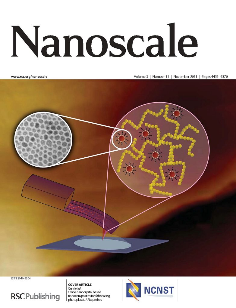
Optical Materials Express. 2011. Vol. 1, num. 2, p. 259 – 269. DOI : 10.1364/OME.1.000259.Oxide nanocrystal based nanocomposites for fabricating photoplastic AFM probes
Nanoscale. 2011. Vol. 3, p. 4632 – 4639. DOI : 10.1039/c1nr10487j.Robust PECVD SiC membrane made for stencil lithography
Microelectronic Engineering. 2011. Vol. 88, p. 2790 – 2793. DOI : 10.1016/j.mee.2010.11.056.Ultra-low power palladium-coated MEMS resonators for hydrogen detection under ambient conditions
2011. 16th International Conference on Solid-State Sensors, Actuators and Microsystems (TRANSDUCERS), Beijing, China, 5-9 June, 2011. p. 787 – 790. DOI : 10.1109/TRANSDUCERS.2011.5969266.A fully integrated IQ-receiver for NMR microscopy
Journal of Magnetic Resonance. 2011. Vol. 209, p. 1 – 7. DOI : 10.1016/j.jmr.2010.12.005.SiN membranes with submicrometer hole arrays patterned by wafer-scale nanosphere lithography
Journal of Vacuum Science & Technology B. 2011. Vol. 29, num. 2, p. 021012/1 – 5. DOI : 10.1116/1.3554404.Fluorophore-doped xerogel antiresonant reflecting optical waveguides
Optics Express. 2011. Vol. 19, num. 6, p. 5026 – 5039. DOI : 10.1364/OE.19.005026.Fabrication and characterization of Silicon Carbide nanostencils
2011.New inks for the direct drop-on-demand fabrication of polymer lenses
2011. 36th International Conference on Micro & Nano Engineering (MNE), Genoa, Italy, September 19-22, 2010. p. 2174 – 2179. DOI : 10.1016/j.mee.2010.12.004.Characterization of Hydrophobic Forces for in Liquid Self-Assembly of Micron-Sized Functional Building Blocks
2011. 2010 MRS Fall Meeting, Boston, Massachusetts, USA, November 30-December 2, 2010. DOI : 10.1557/opl.2011.466.Vertically-Stacked Si Nanowire FETs with sub-micrometer Gate-All-Around polysilicon gates patterned by nanostencil lithography
2011. 37th International Conference on Micro and Nano Engineering (MNE), Berlin, Germany, September 19-23, 2011.GOLD MEMBRANES WITH LARGE ARRAYS OF SUB-µm HOLES FABRICATED BY WAFER-SCALE NANOSPHERE LITHOGRAPHY
The 16th International Conference on Solid-State Sensors, Actuators and Microsystems, Beijing, China, June 5-9, 2011.The effects of channel length and film microstructure on the performance of pentacene transistors
Organic Electronics. 2011. Vol. 12, num. 2, p. 336 – 340. DOI : 10.1016/j.orgel.2010.12.004.Nanoelectromechanical systems (NEMS)
E-nano newsletter. 2011. Vol. 24, p. 37 – 59.Ink-jet printing assisted micro-transfer moulding
MNE 2011, Berlin, September 19-23.Solid-state Nanopore Array Membranes Patterned by Electron Beam Lithography, Nanosphere Lithography and Aluminum Anodization
2011. 8th International Conference on Multi-Material Micro Manufacture (4M 2011)’, u’8th International Conference on Multi-Material Micro Manufacture (4M 2011)’]. p. 225 – 229. DOI : 10.3850/978-981-07-0319-6_200.Drawing with Nanostencils on Flexible Substrates
The 55th International conference on electron, ion, and photon beam technology and nanofabrication” (EIPBN), Las Vegas, NE, USA, May 31 -June 3, 2011.Use of Vertically-Aligned Carbon Nanotube Array to Enhance the Performance of Electrochemical Capacitors
2011. IEEE Nano, Portland, Oregon, USA, August 15-18 2011. p. 80 – 85. DOI : 10.1109/NANO.2011.6144354.Solid-state nanopore array membranes patterned by electron beam lithography, nanosphere lithography and aluminum anodization
4M 2011 Conference, Stuttgart, Germany, November 8-10, 2011.Inkjet printing of SU-8 for high-aspect ratio spherical polymeric microstructures
Swiss-eprint, Basel, Switzerland, December, 1-2, 2011.Localized Ion Implantation Through Micro/Nanostencil Masks
IEEE Transactions on Nanotechnology. 2011. Vol. 10, num. 5, p. 940 – 946. DOI : 10.1109/TNANO.2010.2090171.Ambipolar silicon nanowire FETs with stenciled-deposited metal gate
Microelectronic Engineering. 2011. Vol. 88, num. 8, p. 2732 – 2735. DOI : 10.1016/j.mee.2010.12.117.Dynamic stencil lithography on flexible substrates on full wafer scale
2011.2010
Stress Engineered Thin Films For Life Science Applications
2010.SPM Measurements of Hydrophobic Interactions
Nano-Tera.ch Annual Plenary Meeting, Bern, Switzerland, April 29, 2010.The transition in hydrogen sensing behavior in non-continuous palladium films
Applied Physics Letters. 2010. Vol. 97, num. 12, p. 121911. DOI : 10.1063/1.3491263.Pd-functionalized MEMS resonator for hydrogen gas sensing
Nano-Tera Annual Plenary Meeting, Bern, Switzerland, April 29, 2010.Development of stencil lithography for nanopatterning and for electronic and biosensing applications
Lausanne, EPFL, 2010.Nanoporous SiN membranes patterned by wafer-scale nanosphere lithography
2010. EIPBN’2010. The 54th International Confrence on Electron, Ion, Photon Beam Technology and Nanofabrication., Anchorage, Alaska, U.S.A., June 1-4, 2010.High-resolution microscopy and photolithography devices using focusing micromirrors
EP2389606; US2016091799; US9075227; US2011300490; EP2389606; WO2010084478; WO2010084478.
2010.Magnetic nanocrystal modified epoxy photoresist for microfabrication of AFM probes
2010. MEMSWAVES 2010 and MEMS, Italy, 2010. p. 580 – 584.Silicon nanowire AFM tips grown on released scanning probe cantilevers from stencil-deposited catalysts
2010. M36th International Conference on Micro & Nano Engineering (MNE’2010), Genova, Italy, September 19-22, 2010.Direct write laser at visible wavelength for patterning of high aspect ratio epoxy materials
2010. EIPBN- The 54th International Confrence on Electron, Ion, Photon Beam Technology and Nanofabrication, Anchorage, Alaska, USA, June 1-4, 2010.Fast and robust hydrogen sensors based on discontinuous palladium films on polyimide, fabricated on a wafer scale
Nanotechnology. 2010. Vol. 21, num. 50, p. 505501. DOI : 10.1088/0957-4484/21/50/505501.Three-level Stencil Alignment Fabrication of a High-k Gate Stack Organic Thin Film Transistor
36th International Conference on Micro & Nano Engineering (MNE), Genoa, Italy, September 19-22, 2010.Double-gate pentacene thin-film transistor with improved control in sub-threshold region
Solid-State Electronics. 2010. Vol. 54, num. 9, p. 1003 – 1009. DOI : 10.1016/j.sse.2010.04.019.Organic Thin Film Transistors on Flexible Polyimide Substrates Fabricated by Full Wafer Stencil Lithography
Sensors and Actuators A. 2010. Vol. 162, num. 2, p. 155 – 159. DOI : 10.1016/j.sna.2010.04.016.Flexible Membranes Improve Resolution in Stencil Lithography
The 54th International Conference on Electron, Ion, and Photon Beam Technology, & Nanofabrication, Anchorage, Alaska, U.S.A., June 1- 4, 2010.Direct polymer patterning by high energy reactive ion beam through stencil masks
2010. Micro and Nano Engineering (MNE) 2010, Genova, Italy, September 19-22, 2010.Mechanically tuneable microoptical structure based on PDMS
Sensors and Actuators a-Physical. 2010. Vol. 162, num. 2, p. 260 – 266. DOI : 10.1016/j.sna.2010.02.025.Ambipolar silicon nanowire FETs with stenciled sub-µm metal gate
2010. 36th International Conference on Micro and Nano Engineering (MNE 2010), Genova, Italy, September 19-22, 2010.Fabrication of Metallic Nanodots by Stencil Lithography for Localized Surface Plasmon Resonance Biosensing
Functionalized Plasmonic Nanostructures for Biosensing, Ascona, Switzerland, April 18-23, 2010.Inexpensive and fast wafer-scale fabrication of nanohole arrays in thin gold films for plasmonics
Nanotechnology. 2010. Vol. 21, num. 20, p. 205301. DOI : 10.1088/0957-4484/21/20/205301.System for aligning patterns on a substrate using stencil lithography
ES2332082; WO2010010224; ES2332082.
2010.Direct writing laser of high aspect ratio epoxy microstructures
Journal of Micromechanics and Microengineering. 2010. Vol. 21, num. 1, p. 017003. DOI : 10.1088/0960-1317/21/1/017003.Organic Pentacene Thin Film Transistors on Flexible Substrates Fabricated by Stencil Lithography
Lausanne, EPFL, 2010.Fluidic microstructuring of alginate hydrogels for the single cell niche
Lab on a Chip. 2010. Vol. 10, num. 20, p. 2771 – 2777. DOI : 10.1039/c004988c.Granular Co-C nano-Hall sensors by focused-beam-induced deposition
Nanotechnology. 2010. Vol. 21, num. 11, p. 115503. DOI : 10.1088/0957-4484/21/11/115503.Surface-Tension-Driven Self-Assembly of Filled Cylinders with Different Geometry
Nano-Tera.ch Annual Plenary Meeting, Bern, Switzerland, April 29, 2010.Millimeter waves for NMR enhancement
2010. 35th Int. Conference on Infrared, Millemeter and Terahertz Waves (IRMMW-THz 2010), 2010. DOI : 10.1109/ICIMW.2010.5612362.Wafer-Scale Fabrication of Thin SiN Membranes and Au Films and Membranes with Arrays of Sub-um Holes Using Nanosphere Lithography
Lausanne, EPFL, 2010.High-density, high-aspect ratio epoxy microstructures by Direct Write Laser Patterning
2010. 36th International Conference on Micro & Nano Engineering (MNE), Genoa, Italy, September 19-22, 2010.Design and characterization of low aspectratio nanopore arrays
2010.Metallic Nanodot Arrays Fabricated by Stencil Lithography on SiO2 and Polymer Substrates
The 54th International Conference on Electron, Ion, and Photon Beam Technology, & Nanofabrication, Anchorage, Alaska, U.S.A., June 1-4, 2010.Modeling Self-Assembly at All Scales
Nano-Tera.ch Annual Plenary Meeting, Bern, Switzerland, April 29, 2010.Pd-functionalized MEMS resonator for hydrogen gas sensing at ambient pressure
7th International Workshop on Nanomechanical Cantilever Sensors, Banff, Canada., May 26-28, 2010.Stenciled conducting bismuth nanowires
Journal of Vacuum Science & Technology B: Microelectronics and Nanometer Structures. 2010. Vol. 28, num. 1, p. 169 – 172. DOI : 10.1116/1.3292630.Large arrays of chemo-mechanical nanoswitches for ultralow-power hydrogen sensing
Journal of Micromechanics and Microengineering. 2010. Vol. 20, p. 105019. DOI : 10.1088/0960-1317/20/10/105019.Sputtering of (001)AlN thin films: Control of polarity by a seed layer
Journal of Vacuum Science & Technology B: Microelectronics and Nanometer Structures. 2010. Vol. 28, num. 6, p. L61. DOI : 10.1116/1.3501117.Very Large Scale Arrays of Chemo-Mechanical Nano-Switches for Ultralow Power Hydrogen Sensing
2010. 23rd International IEEE Conference on Micro Electro Mechanical Systems MEMS’2010, Hong Kong, 24-28 January, 2010. DOI : 10.1109/MEMSYS.2010.5442547.Optical transmission properties of corrugated nanoscale hole arrays in thin gold films
2010. Micro and Nano Engineering (MNE) 2010, Genova, Italy, September 19-22, 2010.MAGNETIC NANOCRYSTAL MODIFIED EPOXY PHOTORESIST FOR MICROFABRICATION OF AFM PROBES
MEMSWAVES 2010 and MEMS, Italy, 2010.Use of Force Spectroscopy to Investigate the Adhesion of Living Adherent Cells
Langmuir. 2010. Vol. 26, num. 11, p. 8180 – 8186. DOI : 10.1021/la904526u.2009
Mechanical Hydrogen Sensing
2009.Organic Thin Film Transistors on Flexible Polyimide Substrates Fabricated by Full Wafer Stencil Lithography
2009. XXIII Eurosensors Conference, Lausanne, Switzerland, September 6-9, 2009.. DOI : 10.1016/j.proche.2009.07.190.Drop-On-Demand Inkjet Printing of SU-8 Polymer
Micro and Nanosystems. 2009. Vol. 1, num. 1, p. 63 – 67. DOI : 10.2174/1876402910901010063.Focused Ion Beam: A Versatile Technique for the Fabrication of Nano-Devices
Praktische Metallographie-Practical Metallography. 2009. Vol. 46, num. 3, p. 154 – 156.Double-Gate Pentacene TFTs with Improved Control in Subthreshold Region
2009. 39th European Solid-State Device Research Conference (ESSDERC), Athens, Greece, September 14-18, 2009. p. 205 – 208. DOI : 10.1109/ESSDERC.2009.5331352.Structured ZnO-based contacts deposited by non-reactive rf magnetron sputtering on ultra-thin SiO2/Si through a stencil mask
2009. 2nd International Symposium on Transparent Conductive Oxides, Hersonissos, Crete, Greece, October 22 – 26 2008. p. 1044 – 1047. DOI : 10.1016/j.tsf.2009.03.232.NEMS/CMOS sensor for monitoring deposition rates in stencil lithography
2009. Eurosensor XXIII conference, Lausanne, Switzerland, September 6-9, 2009. p. 425 – 428. DOI : 10.1016/j.proche.2009.07.106.Analysis of the blurring in stencil lithography
Nanotechnology. 2009. Vol. 20, num. 41, p. 415303. DOI : 10.1088/0957-4484/20/41/415303.Large area hole arrays fabricated by a templating method for refractive index sensing
Fourth International Conference on Surface Plasmon Photonics (SPP4), Amsterdam, The Netherlands, June 21-26, 2009.Nanostencil and InkJet Printing for Bionanotechnology Applications
2009. Nano-Net 2009, 4th International ICST Conference on Nano-Networks, Luzern, Switzerland, October 18-20, 2009..Longitudinal detection of ferromagnetic resonance using x-ray transmission measurements
Review of Scientific Instruments. 2009. Vol. 80, num. 12, p. 123902. DOI : 10.1063/1.3267192.Mechanically tuneable microoptical structure based on PDMS
2009. XXIII Eurosensors Conference, Lausanne, Switzerland, September 6-9, 2009.. p. 560 – 563. DOI : 10.1016/j.proche.2009.07.140.Minimized Blurring in Stencil Lithography using a Compliant Membrane
2009. 15th International Conference on Solid-State Sensors, Actuators and Microsystems (Transducers), Denver, USA, 2009.. DOI : 10.1109/SENSOR.2009.5285768.Stencilled Conducting Bismuth Nanowires
2009. 53rd International Conference on Electron, Ion and Photon Beam Technology and Nanofabrication, Marco Island, FL, USA, May 26-29, 2009. DOI : 10.1116/1.3292630.All through stencil MOSFET fabrication
Fall meeting of the American Vacuum Society (AVS), San Jose, CA, USA, 2009.High-Fidelity Printing Strategies for Printing 3D Vascular Hydrogel Structures
2009. 25th International Conference on Digital Printing Technologies, Louisville, KY, Sep 20-24, 2009. p. 411 – 414.Minimized Blurring in Stencil Lithography using a Compliant Membrane
The 15th International Conference on Solid-State Sensors, Actuators and Microsystems (Transducers 2009), Denver, Colorado, USA, June 21-25 2009.A Low-Noise CMOS Receiver Frontend for NMR-based Surgical Guidance
2009. 13th International Conference on Biomedical Engineering (ICBME), Singapore, SINGAPORE, Dec 03-06, 2008. p. 89 – 93. DOI : 10.1007/978-3-540-92841-6_22.Microcollimator for Micrometer-Wide Stripe Irradiation of Cells Using 20–30 keV X Rays
Radiation Research. 2009. Vol. 172, num. 2, p. 252 – 259. DOI : 10.1667/RR1483.1.Drop-on-demand inkjet printing of highly luminescent CdS and CdSe@ZnS nanocrystal based nanocomposites
Microelectronic Engineering. 2009. Vol. 86, p. 1124 – 1126. DOI : 10.1016/j.mee.2008.11.028.Hydrogen sensors based on palladium micro- and nanostructures for fuel cell applications
Lausanne, EPFL, 2009.Nanomechanical Mass Sensor for Spatially Resolved Ultrasensitive Monitoring of Deposition Rates in Stencil Lithography
Small. 2009. Vol. 5, p. 176 – 180. DOI : 10.1002/smll.200990007.Analysis and Applications of Nanostructures Created by Stencil Lithography
2009. 15th International Conference on Solid-State Sensors, Actuators and Microsystems (Transducers), Denver, USA, 2009. DOI : 10.1109/SENSOR.2009.5285463.Stress and aging minimization in photoplastic AFM probes
Microelectronic Engineering. 2009. Vol. 86, num. 4-6, p. 1226 – 1229. DOI : 10.1016/j.mee.2008.12.033.An Oligomerized 53BP1 Tudor Domain Suffices for Recognition of DNA Double-Strand Breaks
Molecular and Cellular Biology. 2009. Vol. 29, p. 1050 – 1058. DOI : 10.1128/MCB.01011-08.Inkjet-Printed Multicolor Arrays of Highly Luminescent Nanocrystal-Based Nanocomposites
Small. 2009. Vol. 5, p. 1051 – 1057. DOI : 10.1002/smll.200801315.Direct Etching of High Aspect structures through a Stencil
2009. MEMS 2009, Sorrento, Italy, January 25-29, 2009. DOI : 10.1109/MEMSYS.2009.4805339.Fluidic-mediated self-assembly for hybrid functional micro/nanosystems (SELFSYS)
Atelier LEA à Arc-et-Senans, Arc-et-Senans, France, September 8-9, 2009.Nanomechanical mass sensor for monitoring deposition rates through confined apertures
The 4th Annual IEEE International Conference on Nano/Micro Engineered and Molecular Systems (NEMS), Shenzhen, China, January 5-8, 2009.Double-resonant x-ray and microwave absorption: Atomic spectroscopy of precessional orbital and spin dynamics
Physical Review B. 2009. Vol. 79, num. 22, p. 224425. DOI : 10.1103/PhysRevB.79.224425.99% random telegraph signal-like noise in gold nanoparticle mu-stripes
Nanotechnology. 2009. Vol. 20, num. 35, p. 355303. DOI : 10.1088/0957-4484/20/35/355303.A single-chip array of NMR receivers
Journal of Magnetic Resonance. 2009. Vol. 201, p. 239 – 249. DOI : 10.1016/j.jmr.2009.09.019.Direct Fabrication of Polymer Micro lens Arrays having Tunable Optical Properties using Drop-On-Demand Ink-Jet Printing Technology
2009. 25th International Conference on Digital Printing Technologies, Louisville, KY, Sep 20-24, 2009. p. 803 – 805.Nanotechnology impact on sensors
Nanotechnology. 2009. Vol. 20, num. 43, p. 430206. DOI : 10.1088/0957-4484/20/43/430206.Conduction in rectangular quasi-one-dimensional and two-dimensional random resistor networks away from the percolation threshold
Physical Review E. 2009. Vol. 80, num. 2, p. 021104. DOI : 10.1103/Physreve.80.021104.Quick and Clean: Stencil Lithography for Wafer-Scale Fabrication of Superconducting Tunnel Junctions
IEEE Transactions on Applied Superconductivity. 2009. Vol. 19, num. 3, p. 242 – 244. DOI : 10.1109/TASC.2009.2019075.Analysis and Applications of Nanostructures Created by Stencil Lithography
The 15th International Conference on Solid-State Sensors, Actuators and Microsystems (Transducers 2009), Denver, Colorado, USA, June 21-25, 2009.2008
Research activities at LMIS1-EPFL
5th NAMIS International workshop, Freiburg, Germany, April 4th-5th, 2008.KFM detection of quantified charges injected into a thin SiO2 layer containing Si nps embedded by ultra low energy ion implantation using stencil lithography
2008. European Materials Research Society (EMRS 2008): Symposium H: Materials and emerging technologies for non-volatile-memory devices, Strasbourg, France, June 26-30 2008..Fabrication of Highly Ordered Vertical Nanogap Arrays and Networks on a Large Scale
34th International Conference on Micro- and Nano Engineering 2008 (MNE 2008), Athens, Greece, September 15-18, 2008.Crystalline silicon cantilevers for piezoresistive detection of biomolecular forces
Microelectronic Engineering. 2008. Vol. 85, num. 5-6, p. 1120 – 1123. DOI : 10.1016/j.mee.2008.01.082.Fabrication of 150 nm half-pitch grating templates for nanoimprint lithography
Journal of Nanoscience and Nanotechnology. 2008. Vol. 9, num. 2, p. 1437 – 1440. DOI : 10.1166/jnn.2009.C173.Detection of bacteria based on the thermomechanical noise of a nanomechanical resonator: origin of the response and detection limits
Nanotechnology. 2008. Vol. 19, num. 3, p. 035503. DOI : 10.1088/0957-4484/19/03/035503.The gas flow rate increase obtained by an oscillating piezoelectric actuator on a micronozzle
Sensors and Actuators A. 2008. Vol. 144, p. 154 – 160. DOI : 10.1016/j.sna.2007.12.024.Single-chip detector for electron spin resonance spectroscopy
Review of Scientific Instruments. 2008. Vol. 79, p. 094105. DOI : 10.1063/1.2969657.The systematic tunability of nanoparticle dimensions through the controlled loading of surface-deposited diblock copolymer micelles
Nanotechnology. 2008. Vol. 19, p. 175301. DOI : 10.1088/0957-4484/19/17/175301.Two-dimensional magnetic resonance force microscopy using full-volume Fourier and Hadamard encoding
Physical Review B. 2008. Vol. 78, p. 214401 (5 pages). DOI : 10.1103/PhysRevB.78.214401.Metallic Nanowires by Full Wafer Stencil Lithography
Nano Letters. 2008. Vol. 8, num. 11, p. 3675 – 3682. DOI : 10.1021/nl801778t.Controlled synthesis of silicon nanocrystals into a thin SiO2 layer synthesized by stencil-masked ultra-low energy ion implantation
2008. French Symposium on Emerging Technologies for Micro-nanofabrication, Toulouse, France, November 19-21, 2008.Design and optimization of nanogap array sensors
Eurosensors XXII, Dresden, Germany, September 7-10, 2008.Charging dynamics of localized 2D layers of Si nanocrystals embedded into SiO2 by stencil masked ultra low energy ion implantation process
European Materials Research Society (EMRS 2008): Symposium H: Materials and emerging technologies for non-volatile-memory devices, Strasbourg, France, June 26-30 2008.Novel methods to pattern polymers for microfluidics
2008. 33rd International Conference on Micro- and Nano Engineering 2007 (MNE 2007), Copenhagen, Denmark, 23-26 Sept, 2007. p. 972 – 975. DOI : 10.1016/j.mee.2008.01.052.Silicon nanoparticles synthesized in SiO2 pockets by stencil-masked low energy ion implantation and thermal annealing
2008. Meeting of the European-Materials-Research-Society, Strasbourg, FRANCE, May 28-Jun 01, 2007. p. 395 – 401. DOI : 10.1016/j.spmi.2007.12.013.Compact CMOS current conveyor for integrated NEMS resonators
Iet Circuits Devices & Systems. 2008. Vol. 2, p. 317 – 323. DOI : 10.1049/iet-cds:20070320.Ink-jet printing of highly luminescent nanocrystal/polymer nanocomposites for microstructure fabrication: effect of the ink parameters
34th International Conference on Micro- and Nano Engineering 2008 (MNE 2008), Athens, Greece, September 15-18, 2008.A single nanotrench in a palladium microwire for hydrogen detection
Nanotechnology. 2008. Vol. 19, num. 12, p. 125502. DOI : 10.1088/0957-4484/19/12/125502.Novel methods to pattern polymers for microfluidics
Microelectronic Engineering. 2008. Vol. 85, p. 972 – 975. DOI : 10.1016/j.mee.2008.01.052.Inkjet printing and high aspect ratio structuring for polymer-based micro and nano systems
Lausanne, EPFL, 2008.Full-wafer fabrication by nanostencil lithography of micro/nanomechanical mass sensors monolithically integrated with CMOS
Nanotechnology. 2008. Vol. 19, num. 30, p. 305302. DOI : 10.1088/0957-4484/19/30/305302.Pentacene – SiO2 interface: role of the environment prior to pentacene deposition and its impact on TFT DC characteristics
26th International Conference on Microelectronics, Nis, Serbia, May 11-14 2008.Element-resolved x-ray ferrimagnetic and ferromagnetic resonance spectroscopy
New Journal of Physics. 2008. Vol. 10, p. 013011. DOI : 10.1088/1367-2630/10/1/013011.Optical Transmission Properties of Corrugated Nanoscale Hole Arrays in Thin Gold Films
2008. 34th International Conference on Micro- and Nano Engineering 2008, Athens, Greece, Sept 15-18, 2008.Discontinuous Palladium Nanostructures for H2 Sensing
Pacific Rim Meeting on Electrochemical and Solid-State Science (PRIME2008), Honolulu, Hawaii, October 12-17 2008.Bismuth nanowires with stencil lithography
2008. 34th International Conference on Micro and Nano Engineering 2008 (MNE 2008), Athens, Greece, September 15-18, 2008..Design and optimization of nanogap array sensors
Eurosensors XXII, Dresden, Germany, October 7-10, 2008.Direct fabrication of NIL stamps using Stencil Lithography
Eurosensors XXII, Dresden, Germany, September 7-10, 2008.Hydrogen Sensors based on Nanoscaled Discontinuities in Palladium
NAMIS International autumn school, Tokyo, Japan, September 2008.Stencil Lithography: Quick and Clean
Smart Systems Integration (SSI), Barcelona, Spain, 2008.Inkjet printing of SU-8 for polymer-based MEMS: A case study for microlenses
21st IEEE International Conference on Micro Electro Mechanical Systems (MEMS 2008), Tucson, USA, 13-17 January, 2008.Development of novel SU-8 based nanoimprint lithography
2008. The 9th International Conference on Solid-State and Integrated-Circuit Technology (ICSICT), Beijing, China, October 20-23, 2008.Stencil assisted reactive ion etching for micro and nano patterning
Microelectronic Engineering. 2008. Vol. 85, num. 8, p. 1705 – 1708. DOI : 10.1016/j.mee.2008.04.027.Resistless ion implantation of sub-micron scale features through nano-stencil
34th International Conference on Micro- and Nano Engineering 2008 (MNE 2008), Athens, Greece, September 15-18, 2008.Electron counting at room temperature in an avalanche bipolar transistor
Applied Physics Letters. 2008. Vol. 92, num. 2, p. 022111. DOI : 10.1063/1.2830015.Optical transmission properties of corrugated nanoscale hole arrays in thin gold films
34th International Conference on Micro- and Nano Engineering 2008 (MNE 2008), Athens, Greece, Sept 15-18, 2008.Discontinuous Palladium Nanostructures for H2 Sensing
2008. ECS Transactions, Hawaii, 2008. p. 457 – 463. DOI : 10.1149/1.2981151.Dynamic Stencil Lithography on Full Wafer Scale
The 52nd International Conference on Electron, Ion, and Photon Beam Technology and Nanofabrication (EIPBN 2008), Portland, Oregon, May 27–30, 2008.Combining micelle self-assembly with nanostencil lithography to create periodic/aperiodic micro- /nanopatterns on surfaces
Advanced Materials. 2008. Vol. 20, num. 18, p. 3533 – 3538. DOI : 10.1002/adma.200702478.UV-curable nanoimprint resin with enhanced anti-sticking property
Applied Surface Science. 2008. Vol. 254, p. 4793 – 4796. DOI : 10.1016/j.apsusc.2008.01.095.Pentacene – SiO2 interface: Role of the environment prior to pentacene deposition and its impact on TFT DC characteristics
2008. 26th International Conference on Microelectronics (MIEL 2008), Nis, Serbia, May 11-14, 2008. DOI : 10.1109/ICMEL.2008.4559282.Quick and Clean: Stencil Lithography for Wafer-Scale Fabrication of Superconducting Tunnel Junctions
2008. Applied Superconductivity Conference 2008 (ASC 2008), Chicago, Illinois USA, August 17-22 2008. DOI : 10.1109/TASC.2009.2019075.Direct fabrication of NIL stamps using Stencil Lithography
Eurosensors XXII, Dresden, Germany, September 7-10, 2008.A nanoimprint lithography for fabricating SU-8 gratings for near-infrared to deep-UV application
Microelectronic Engineering. 2008. Vol. 85, p. 914 – 917. DOI : 10.1016/j.mee.2008.01.072.Drop-on-demand Ink-jet printing of functional materials: Case studies of SU-8 and NCs-embedded Polymer nanocomposites
International Conference on Digital Fabrication Technologies, Pittsburgh, Pennsylvania, USA, September 7-12, 2008.Nanostructured ZnO-based layers deposited by non reactive rf magnetron sputtering on ultra-thin SiO2/Si through a stencil mask
2nd International Symposium on Transparent Conductive Oxides, Hersonissos, Crete, Greece, October 22 – 26 2008.Direct fabrication of NEMS by etching through Stencil
Micro Nano cantilever Sensors 2008 (MNCS 08), Mainz, Germany, May 19-21, 2008.Resistivity Measurements of Gold Wires Fabricated by Stencil Lithography on Flexible Polymer Substrates
2008. 33rd International Conference on Micro- and Nano Engineering 2007 (MNE 2007), Copenhagen, Denmark, 23-26 Sept, 2007. p. 1108 – 1111. DOI : 10.1016/j.mee.2007.12.069.Stress and aging minimization in photoplastic AFM probes
34th International Conference on Micro and Nano Engineering 2008 (MNE 2008), Athens, Greece, September 15-18, 2008.Sub-100 nm-scale Aluminum Nanowires by Stencil Lithography: Fabrication and Characterization
2008. 3rd IEEE International Conference of Nano/Micro Engineered and Molecular Systems, Sanya, Hainan Island, China, January 6-9, 2008.. p. 807 – 811. DOI : 10.1109/NEMS.2008.4484447.Etching of sub-micrometer structures through Stencil
2008. 33rd International Conference on Micro- and Nano Engineering 2007 (MNE 2007), 23-26 Sept, 2007, Copenhagen, Denmark, Copenhagen, Denmark, 23-26 Sept, 2007. p. 1010 – 1014. DOI : 10.1016/j.mee.2007.12.068.Inkjet printing of SU-8 for polymer-based MEMS a case study for microlenses
2008. 21st IEEE International Conference on Micro Electro Mechanical Systems 2008, Tucson, Arizona, USA, Jan 13-17, 2008. p. 407 – 410. DOI : 10.1109/MEMSYS.2008.4443679.Dynamic Stencil Lithography on Full Wafer Scale
2008. 52nd International Conference on Electron, Ion, and Photon Beam Technology and Nanofabrication (EIPBN 2008), Portland, Oregon, May 27–30, 2008.Ion Beam Etching: Replication of Micro Nano-structured 3D Stencil Masks
2008. 20th International Conference on the Application of Accelerators in Research and Industry (CAARI), Fort Worth, USA, 2008. p. 539 – 541. DOI : 10.1063/1.3120093.Dynamic stencil lithography on full wafer scale
Journal of Vacuum Science and Technology B. 2008. Vol. 26, p. 2054 – 2058. DOI : 10.1116/1.2987953.Nanopatterned Self-Assembled Monolayers by Using Diblock Copolymer Micelles as Nanometer-Scale Adsorption and Etch Masks
Advanced Materials. 2008. Vol. 20, num. 10, p. 1962 – 1965. DOI : 10.1002/adma.200702005.Stress and aging minimization in photoplastic AFM probes
2008. 34th International Conference on Micro and Nano Engineering 2008 (MNE 2008), Athens, Greece, September 15-18, 2008. DOI : 10.1016/j.mee.2008.12.033.KFM detection of quantified charges injected into a thin SiO2 layer containing Si nps embedded by ultra low energy ion implantation using stencil lithography
European Materials Research Society (EMRS 2008): Symposium H: Materials and emerging technologies for non-volatile-memory devices, Strasbourg, France, June 26-30 2008.Charging dynamics of localized 2D layers of Si nanocrystals embedded into SiO2 by stencil masked ultra low energy ion implantation process
2008. European Materials Research Society (EMRS 2008): Symposium H: Materials and emerging technologies for non-volatile-memory devices, Strasbourg, France, June 26-30 2008..Controlled synthesis of silicon nanocrystals into a thin SiO2 layer synthesized by stencil-masked ultra-low energy ion implantation
French Symposium on Emerging Technologies for Micro-nanofabrication, Toulouse, France, November 19 – 21 2008.Mechanical stabilisation and design optimisation of masks for stencil lithography: Numerical approach and experimental validation
Microelectronic Engineering. 2008. Vol. 85, p. 2243 – 2249. DOI : 10.1016/j.mee.2008.07.009.Bismuth nanowires with stencil lithography
34th International Conference on Micro and Nano Engineering 2008 (MNE 2008), Athens, Greece, September 15-18, 2008.Quick and Clean: Stencil Lithography for Wafer-Scale Fabrication of Superconducting Tunnel Junctions
Applied Superconductivity Conference 2008 (ASC 2008), Chicago, Illinois USA, August 17-22 2008.Nanophotonic crystals with chiral elements by a hot embossing process in SU-8
Microelectronic Engineering. 2008. Vol. 85, p. 866 – 869. DOI : 10.1016/j.mee.2007.12.085.Magnetic Nanocrystals Modified Epoxy Photoresist for fabrication of NEMS and MEMS
2008. 34th International Conference on Micro and Nano Engineering (MNE’2008), Athens, Greece, September 15-18, 2008.Etching of sub-micrometer structures through Stencil
Microelectronic Engineering. 2008. Vol. 85, p. 1010 – 1014. DOI : 10.1016/j.mee.2007.12.068.Drop-on-demand Ink-jet printing of functional materials: Case studies of SU-8 and NCs-embedded Polymer nanocomposites
2008. International Conference on Digital Fabrication Technologies, Pittsburgh, Pennsylvania, USA, September 7-12, 2008..Tunable, high aspect ratio pillars on diverse substrates using copolymer micelle lithography: an interesting platform for applications
Nanotechnology. 2008. Vol. 19, num. 28, p. 285301. DOI : 10.1088/0957-4484/19/28/285301.Reusability of nanostencils for the patterning of Aluminum nanostructures by selective wet etching
Microelectronic Engineering. 2008. Vol. 85, num. 5-6, p. 1237 – 1240. DOI : 10.1016/j.mee.2007.12.083.2007
Fabrication and testing of a poly(vinylidene fluoride) (PVDF) microvalve for gas flow control
Smart Materials and Structures. 2007. Vol. 16, p. 2302 – 2307. DOI : 10.1088/0964-1726/16/6/033.Highly Sensitive Cantilevers, with and without Magnetic Tip, for Magnetic Resonance Force Microscopy
2007. 14th International Conference on Solid-State Sensors, Actuators and Microsystems (Transducers ’07), Lyon, France, June 10-14 , 2007. p. 1537 – 1540. DOI : 10.1109/SENSOR.2007.4300438.Microfabricated electrically conducting and wear-resistant nanoprobes for scanning probe applications
Lausanne, EPFL, 2007.Quick & Clean: Advances in High Resolution Stencil Lithography
E nano newsletter. 2007. Vol. 8, p. 22 – 28.Selective deposition of gold nanoparticles using Van der Waals interactions
physica status solidi (c). 2007. Vol. 4, num. 2, p. 276 – 278. DOI : 10.1002/pssc.200673344.Integrated Nickel Micro-Nano-Hall Sensors on SU-8 Cantilevers for Scanning Hall Probe Microscopy
2007. 14th International Conference on Solid-State Sensors, Actuators and Microsystems (Transducers ’07), Lyon, France, June 10-14, 2007. p. 2589 – 2592. DOI : 10.1109/SENSOR.2007.4300701.Micropositioning and microscopic observation of individual picoliter-sized containers within SU-8 microchannels
Microfluidics and Nanofluidics. 2007. Vol. 3, num. 2, p. 189 – 194. DOI : 10.1007/s10404-006-0119-2.Patterning of parallel nanobridge structures by reverse nanostencil lithography using an edge-patterned stencil
Nanotechnology. 2007. Vol. 18, num. 4, p. 044002. DOI : 10.1088/0957-4484/18/4/044002.Focused electron beam induced deposition of nickel
2007. 51st International Conference on Electron, Ion, and Photon Beam Technology and Nanofabrication, Denver, CO, May 29-Jun 01, 2007. p. 2228 – 2232. DOI : 10.1116/1.2794071.Towards Reliable 100-Nanometer Scale Stencil Lithography on Full Wafer: Progress AND Challenges
2007. 14th International Conference on Solid-State Sensors, Actuators and Microsystems (Transducers ’07), Lyon, France, 10-14 June, 2007. p. 195 – 198. DOI : 10.1109/SENSOR.2007.4300104.Stencil mask for accurate pattern replication
WO2007099518.
2007.The Light at the End of the Tunnel Junction – Improving the Energy Resolution of UV Single-Photon Spectrometers using Diffusion Engineering
Yale University, 2007.Micrometric Droplets Motion
“4th Annual Conference on Foundations of Nanoscience: Self-Assembled Architectures and Devices (FNANO07), Utah, USA, 18-21 April, 2007.Nanostenciling for fabrication and interconnection of nanopatterns and microelectrodes
Applied Physics Letters. 2007. Vol. 90, num. 9, p. 093113. DOI : 10.1063/1.2710473.Integrated Nickel Micro-Hall Sensors on SU-8 Cantilevers for Scanning Hall Probe Microscopy
14th International Conference on Solid-State Sensors, Actuators and Microsystems (Transducers ’07), Lyon, France, 10-14 June, 2007.Towards Reliable 100-Nanometer Scale Stencil Lithography on Full Wafer: Progress AND Challenges
14th International Conference on Solid-State Sensors, Actuators and Microsystems (Transducers ’07), Lyon, France, 10-14 June, 2007.Focused Ion Beam Engineered Nanogap in a Palladium Microwire as a Mechanical Switch for Hydrogen Detection
33rd International Conference on Micro- and Nano Engineering 2007 (MNE 2007), Copenhagen, Denmark, 23-26 Sept, 2007.Highly Sensitive Si Cantilevers, with and without Magnetic Tip, for Magnetic Resonance Force Microscopy
14th International Conference on Solid-State Sensors, Actuators and Microsystems (Transducers ’07), Lyon, France, 10-14 June, 2007.A Compact and Low-Power CMOS Circuit for Fully-Integrated NEMS Resonators
IEEE Transactions on Circuits and Systems II. 2007. Vol. 54, num. 5, p. 377 – 381. DOI : 10.1109/TCSII.2007.892228.Nanostenciling for combinatorial fabrications and interconnections of nanopatterns and microelectrodes
Virtual Journal of Nanoscale Science & Technology. 2007. Vol. 15, num. 10.Enhancing the energy resolution of a singles photon STJ spectrometer using diffusion engineering
IEEE Transactions on Applied Superconductivity. 2007. Vol. 17, num. 2, p. 324 – 327. DOI : 10.1109/TASC.2007.898612.Micro and nano tools for magnetic field imaging
Lausanne, EPFL, 2007.Computational Design and Optimisation of Mechanically Reinforced Masks for Stencil Lithography
EuroSimE 2007, Thermal, Mechanical and Multiphysics Simulation and Experiments in Micro-Electronics and Micro-Systems,, London, UK, 15-18 April, 2007.Direct observation of nuclear spin diffusion in real space
Physics Review Letters. 2007. Vol. 99, p. 227603. DOI : 10.1103/PhysRevLett.99.227603.Micrometric Droplets Motion
2007. 4th Annual Conference on Foundations of Nanoscience: Self-Assembled Architectures and Devices (FNANO07), Utah, USA, 18-21 April, 2007.Etching of sub-micrometer structures through Stencil
33rd International Conference on Micro- and Nano Engineering 2007 (MNE 2007), Copenhagen, Denmark, 23-26 Sept, 2007.Fabrication of planar chiral photonic meta-materials on SU- 8 using nanoimprint lithography technique
2007. International Conference on Nanoscience & Technology (Chinanano), Beijing, China, June 4-6, 2007.Dry etching for the correction of gap-induced blurring and improved pattern resolution in nanostencil lithography
Journal of Microlithography, Microfabrication, and Microsystems. 2007. Vol. 6, p. 013005 – 1. DOI : 10.1117/1.2435273.Uniformly Dispersed Deposition of Colloidal Nanoparticles and Nanowires by Boiling
Applied Physics Letters. 2007. Vol. 91, num. 17, p. 173112. DOI : 10.1063/1.2803320.NMR spectroscopy and perfusion of mammalian cells using surface microprobes
Lab on a Chip. 2007. Vol. 7, num. 3, p. 381 – 383. DOI : 10.1039/B613240E.Cell Patterning Using Nanostencil Lithography: An Alternative to Micro-Contact Printing
BIOSURF VII -Functional Interfaces for Directing Biological Response, Zurich, Switzerland, 29 – 31 August, 2007.Predicting mask distortion, clogging and pattern transfer for stencil lithography
Microelectronic Engineering. 2007. Vol. 81, num. 1, p. 42 – 53. DOI : 10.1016/j.mee.2006.08.003.Reusability of nanostencils for the patterning of Aluminum nanostructures by selective wet etching
33rd International Conference on Micro- and Nano Engineering 2007 (MNE 2007), Copenhagen, Denmark, 23-26 Sept, 2007.Stencil Lithography on Flexible Polymer Substrates
33rd International Conference on Micro- and Nano Engineering 2007 (MNE 2007), Copenhagen, Denmark, 23-26 Sept, 2007.Improved and new properties of resist materials by doping with nanoparticles and nanocrystals
Solutions for the Microsystems Technology Market (Microsys 2007 Congress), Berlin, Germany, 7- 8 March, 2007.An Epoxy Photoresist Modified by Luminescent Nanocrystals for the Fabrication of 3D High-Aspect-Ratio Microstructures
Advanced Functional Materials. 2007. Vol. 17, p. 2009 – 2017. DOI : 10.1002/adfm.200700098.Synthesis of localized 2D-layers of silicon nanoparticles embedded in a SiO2 layer by a stencil-masked ultra-low energy ion implantation process
Physica Status Solidi (a). 2007. Vol. 204, num. 2, p. 487 – 491. DOI : 10.1002/pssa.200673232.Stencil Lithography – Quick & Clean Surface Patterning at Mesoscopic Scales
AVS 54th International Symposium & Exhibision, Seattle, WA, USA, 14-19 October, 2007.2006
Corrugated membranes for improved pattern definition with micro/nanostencil lithography
Sensors and Actuators A. 2006. Vol. 130-131, p. 568 – 574. DOI : 10.1016/j.sna.2005.08.037.Luminescent nanocrystal modified photoresin for fabrication of high-aspect ratio three-dimensional microstructures
2006 MRS Fall Meeting, Boston, USA, 27 Nov – 1 Dec, 2006.Self-Organized Nanostructures on Large Surfaces: A Versatile Toolbox
Annual Meeting of the Swiss Physical Society, Lausanne, Switzerland, 13-14 Feb, 2006.Novel full platinum nanoprobes suitable for biological SPM experiments
2006. 2006 International Conference on Microtechnologies in Medicine and Biology, Okinawa, Japan, 9-12 May, 2006.Self-assembly of tunable, responsive polymer nanostructures : tools for nanofabrication of functional interfaces
Lausanne, EPFL, 2006.REVERSE TRANSFER OF NANOSTENCIL PATTERNS USING INTERMEDIATE SACRIFICIAL LAYER AND LIFT-OFF
2006
MICRO-HALL SENSORS ON SU-8 CANTILEVERS FOR MAGNETIC IMAGINIG
2006
MECHANOSENSITIVE CELL SUBSTRATE
2006
MICROFABRICATED MOLDS FOR INKJET APPLICATIONS
2006
FABRICATION OF NANOAPERTURES ON STENCILS USING FOCUSED ION BEAMS FOR SHADOW MASK EVAPORATION
2006
Dry etching release of polymer-based cantilevers with integrated electrodes
International workshop on nanomechanical sensors, Copenhagen, Denmark, 7-10 May, 2006.SUB-MICRON SCALE PATTERN TRANSFER INTO POLYMERS BY THERMAL IMPRINT LITHOGRAPHY
2006
Full wafer integration of NEMS on CMOS by nanostencil lithography
IEEE International Electron Devices Meeting, San Francisco, USA, 11-13 Dec, 2006,.MONOLITHIC INTEGRATION OF NANOMECHANICAL RESONATORS WITH CMOS CIRCUITRY: FULL-WAFER NANOPATTERNING BY NANOSTENCIL LITHOGRAPHY
2006
Application of Microstencil Lithography on Polymer Surfaces for Microfluidic Systems with Integrated Microelectrodes
International Conference on Microtechnologies in Medicine and Biology, Okinawa, Japan, 9-12 May, 2006.Fabrication and characterisation of ultrasensitive monocrystalline silicon cantilevers with integrated magnetic tips
2006.Full wafer integration of NEMS on CMOS by nanostencil lithography
2006. 2006 IEEE international Electron Devices, Electron Devices Meeting, Electron Devices Meeting, 2006. IEDM ’06. International, December 11-13, San Francisco, U.S.A., December 11-13, 2006. p. 1 – 4. DOI : 10.1109/IEDM.2006.346830.Reverse nanostencil lithography using dual pattern transfer
32nd International Conference on Micro- and Nano Engineering 2006 (MNE 2006), Barcelona, Spain, 17-20 Sept, 2006.Polymer-based cantilevers with integrated electrodes
IEEE Journal of Microelectromechanical Systems. 2006. Vol. 15, num. 4, p. 890 – 895. DOI : 10.1109/JMEMS.2006.879376.SETTING-UP AND EVALUATION OF UV-IMPRINT LITHOGRAPHY
2006
Application of Microstencil Lithography on Polymer Surfaces for Microfluidic Systems with Integrated Microelectrodes
2006. 2006 International Conference on Microtechnologies in Medicine and Biology, Okinawa, Japan, 9-12 May, 2006.Stenci Lithography: Status and Prospectives
International Conference on Nanoscience and Technology ICN&T 2006, Basel, Switzerland, 30 July – 4 Aug, 2006.Interdigital 50 nm Ti Electrode Arrays Fabricated Using XeF2 Enhanced Focused Ion Beam Etching
Nanotechnology. 2006. Vol. 17, num. 11, p. 2722 – 2729. DOI : 10.1088/0957-4484/17/11/002.Combined Al-protection and HF-vapor release process for ultrathin single crystal silicon cantilevers
Microelectronic Engineering. 2006. Vol. 83, num. 4-9, p. 1306 – 1308. DOI : 10.1016/j.mee.2006.01.218.Formation of Metal Nano- and Micro-patterns on Self-Assembled Monolayers Using Pulsed Laser Deposition through Nanostencils and Electroless Deposition
Advanced Functional Materials. 2006. Vol. 16, num. 10, p. 1337 – 1342. DOI : 10.1002/adfm.200500933.ELECTROSTATIC CLAMPING CHUCK FOR NANOSTENCILS
2006
Development of actuators using PVDF piezoelectric polymer
XXIX Brazilian National Meeting of Physics of Condensate Matter (Encontro Nacional de Física da Matéria Condensada), Sao Lourenço, Brazil, 9-13 May, 2006.Reverse transfer of nanostencil patterns using intermediate sacrificial layer and lift-off process
Journal of Vacuum Science and Technology B. 2006. Vol. 24, num. 6, p. 2772 – 2775. DOI : 10.1116/1.2366610.Block copolymer micelles as switchable templates for nanofabrication
Langmuir. 2006. Vol. 22, num. 8, p. 3450 – 3452. DOI : 10.1021/la052299a.Fabrication and functionalization of nanochannels by electron-beam-induced silicon oxide deposition
Langmuir. 2006. Vol. 22, num. 25, p. 10711 – 10715. DOI : 10.1021/la061321c.Chemical patterns of Octadecyltrimethoxysilane monolayers for the selective deposition of gold nanoparticles on silicon substrate
Montpellier 2006 SPM, Sensors and Nanostructures International Conference, Montpellier, France, 3-6 June, 2006.Synthesis of localized 2D-layers of silicon nanoparticles embedded in a SiO2 layer by a stencil-masked ultra-low energy ion implantation process
14th International Conference on Superlattices, Nano-Structures and Nano-Devices, Istanbul, Turkey, 30 July – 4 Aug, 2006.IMPROVED LARGE-AREA AND HIGH-DENSITY NANOSTENCIL LITHOGRAPHY
2006
Realization and characterization of magnetic multilayer for MFM tips
2006.Permalloy thin films exchange-coupled to arrays of stencilled cobalt islands
32nd International Conference on Micro- and Nano Engineering 2006 (MNE 2006), Barcelona, Spain, 17-20 Sept, 2006.Electrically conducting probes with full tungsten cantilever and tip for scanning probe applications
Nanotechnology. 2006. Vol. 17, num. 5, p. 1464 – 1469. DOI : 10.1088/0957-4484/17/5/050.Small AFM cantilevers for biological applications
2006.NANOSCALE DISPENSING OF LIQUIDS WITH AFM-CANTILEVER
2006
STAMP FABRICATION FOR NANOIMPRINT LITHOGRAPHY BY PATTERN DEFINITION WITH STENCIL LITHOGRAPHY
2006
Modelling pattern transfer in stencil lithography
32nd International Conference on Micro- and Nano Engineering 2006 (MNE 2006), Barcelona, Spain, 17-20 Sept, 2006.Silicon Supported Membranes for Improved Large-Area and High-Density Micro/Nanostencil Lithography
IEEE Journal of Microelectromechanical Systems. 2006. Vol. 15, num. 6, p. 1663 – 1670. DOI : 10.1109/JMEMS.2006.885981.FABRICATION OF ULTRA SENSITIVE MONOCRYSTALLINE SILICON CANTILEVERS
2006
Novel full platinum nanoprobes suitable for biological SPM experiments
International Conference on Microtechnologies in Medicine and Biology, Okinawa, Japan, 9-12 May, 2006.Surface micromachining of Ceramic-MEMS based on SU-8 micromoulding of Polyureasilazane
CIMTEC 2006 (11th International Conferences on Modern Materials and Technologies), Sicily, Italy, 4-9 June, 2006.Cell Membranes Suspended Across Nanoaperture Arrays
Langmuir. 2006. Vol. 22, num. 1, p. 22 – 25. DOI : 10.1021/la052387v.Nanostencil Lithography – Quick & Clean: Towards a reliable scalable nanopatterning method
32nd International Conference on Micro- and Nano Engineering 2006 (MNE 2006), Barcelona, Spain, 17-20 Sept, 2006.MICROFABRICATED HALL SENSORS MINIATURIZED TO THE NANOMETER SCALE
2006
Emerging Nanopatterning Methods based on MEMS Technology
Ultimate Lithography and Nanofabrication for Electronics and Life Science (LITHO2006), Marseille, France, 25-30 June, 2006.Full tungsten and platinum nanoprobes for electrically conducting scanning probe methods
Korean MEMS Conference, Jeju, Korea, 6-8 April, 2006.Fabrication of metallic patterns by microstencil lithography on polymer surfaces suitable as microelectrodes in integrated microfluidic systems
Journal of Micromechanics and Microengineering. 2006. Vol. 16, num. 8, p. 1606 – 1613. DOI : 10.1088/0960-1317/16/8/023.Implantable Glucose Sensor, IGLUS III – Membrane Technology –
CTI Medtech Event 2006, Bern, Switzerland, 30 Aug, 2006.Permalloy thin films exchange coupled to arrays of cobalt islands
Applied Physics Letters. 2006. Vol. 89, num. 14, p. 142508. DOI : 10.1063/1.2357007.Surface Micromachining of Polyureasilazane Based Ceramic-MEMS using SU-8 Micromolds
2006. CIMTEC 2006 (11th International Conferences on Modern Materials and Technologies), Sicily, Italy, 4-9 June, 2006. p. 1293 – 1298.Inkjet-Based Deposition of Micro/Nano-Objects on Functional Surfaces – Controlling and Exploiting Self-Assembly across Length-Scales
LEA Laboratoire Européen Associé en Microtechnique, France, 12-13 Sept, 2006,.Integrated Micro Hall Sensor on SU-8 Cantilever
2006.Directed assembling of gold nanoparticles using Van der Waals interactions
14th International Conference on Superlattices, Nano-Structures and Nano-Devices, Istanbul, Turkey, 30 July – 4 Aug, 2006.Photoluminescence characterization of few-nanocrystals electronic devices
Journal of Luminescence. 2006. Vol. 121, num. 2, p. 340 – 343. DOI : 10.1016/j.jlumin.2006.08.070.FABRICATION OF NANOPORES IN SIN MEMBRANES USING FIB
2006
Nanostencil lithography for nanowire patterning
Nanoelectronics Days 2006, Aachen, Germany, 11-13 Oct, 2006.Full platinum nanoprobes for electrically conducting scanning probe methods
The 16th International Microscopy Congress, Sapporo, Japan, 3-8 Sept, 2006.HYBRID SPM PROBE WITH PLATINUM CANTILEVER AND TIP FOR ELECTRICALLY CONDUCTING MODE SPM EXPERIMENTS
2006
High-aspect ratio three-dimensional photoresin-based microstructures doped with luminescent nanocrystals
32nd International Conference on Micro- and Nano Engineering 2006 (MNE 2006), Barcelona, Spain, 17-20 Sept, 2006.Conduction Mechanisms in Organic MOSFETs with Bottom and Top Source and Drain Contacts
36th European Solid-State Device Research Conference, Montreux, Switzerland, 18-22 Sept, 2006.Photoluminescence characterization of localized 2D-layers of few-nanocrystals electronic devices
The E-MRS 2006 Spring Meeting (E-MRS – IUMRS – ICEM 06), Nice, France, 29 May – 2 June, 2006.MEMS-based nanopatterning: new challenges and opportunities for Materials Science
2nd Workshop on Characterization of Materials for MEMS/MST Devices, Tokyo, Japan, 6 Nov.Tuning the Dimensions and Periodicities of Nanostructures Starting from the Same Polystyrene-block-poly(2-vinylpyridine) Diblock Copolymer
Advanced Functional Materials. 2006. Vol. 16, num. 11, p. 1469 – 1475. DOI : 10.1002/adfm.200500524.Stencil lithography : an ancient technique for advanced micro- and nano-patterning
Lausanne, EPFL, 2006.Approach of Top-down technology to self-assembled materials for applications in nano-patterning and various sensing devices
EPFL-IIS-KIMM Joint Workshop on Micro/Nano Mechatronics and Production Technologies, Tokyo, Japan, 16 and 18 Oct, 2006.MICROFABRICATED RECYCLABLE MOULDS FOR FULL-WAFER STRUCTURING OF CERAMIC PRECURSOR POLYMERS
2006
SMALL AFM CANTILEVERS FOR BIOLOGICAL APPLICATION
2006
Full tungsten and platinum nanoprobes for electrically conducting scanning probe methods
2006. The 8th Korean MEMS Conference, Jeju, Korea, 6-8 April, 2006.A Flexible Platform Based on Self-Assembly of Block-Copolymer Micelles to Create Nanotopographies of Tunable Dimensions in Different Materials. Combination with Top-Down Methods and first Applications as Cell Growth Substrates
International Conference on Nanoscience and Technology ICN&T 2006, Basel, Switzerland, 30 July – 4 Aug, 2006.Dynamic Stencil Lithography
2006.Surface Micromachining of Polyureasilazane Based Ceramic-MEMS using SU-8 Micromolds
Advances in Science and Technology. 2006. Vol. 45, p. 1293 – 1298. DOI : 10.4028/www.scientific.net/AST.45.1293.Micro- and nanostructured devices for investigating biomolecular interactions
CHIMIA. 2006. Vol. 60, num. 11, p. 754 – 760. DOI : 10.2533/chimia.2006.754.2005
Methods for rapid prototyping of nanomechanical (NEMS) devices
15th NID Workshop, Madrid, Spain, 31 Jan – 2 Feb, 2005.Ink-Jetting of Polymers and Biomaterials
The 9th Annual European Conference On Micro & Nanoscale Technologies for the Biosciences (Nanotech Montreux 2005), Montreux, Switzerland, 15-17 Nov, 2005.Microscopic four-point probe based on SU-8 cantilevers
Review of Scientific Instruments. 2005. Vol. 76, num. 12, p. 125102 (4 pages). DOI : 10.1063/1.2140443.Surface Nanostructuring through block copolymer self-assembly
2nd BENEFRI Material Day, Neuchatel, Switzerland, 24 June, 2005.NANOINGENEERING OF SIN MEMBRANES USING FIB
2005
Nanocomposites based on luminescent colloidal nanocrystals in polymers: new opportunities for micro and nano fabrication
The 9th Annual European Conference On Micro & Nanoscale Technologies for the Biosciences (Nanotech Montreux 2005), Montreux, Switzerland, 15-17 Nov, 2005.Diffusion-engineered quasiparticle multiplication for STJ single photon detectors
IEEE Transactions on Applied Superconductivity. 2005. Vol. 15, num. 2, p. 609 – 612. DOI : 10.1109/TASC.2005.849956.Micro-Four-Point probe based on SU-8 cantilevers
2005.Microscopic four-point probe (u4PP) based on SU-8 cantilevers
International Conference on Micro- and Nano Engineering 2005 (MNE 2005), Vienna, Austria, 19-22 Sept, 2005.Microscopic four-point probe based on SU-8 cantilevers
Virtual Journal of Nanoscale Science & Technology. 2005. Vol. 12, num. 26.Tunable surface nanostructures from Block copolymer self-assembly
SFC EuroChem 2005, Nancy, France, 28 Aug – 1 Sept, 2005.MEMS tools for combinatorial materials processing and high-throughput characterization
Measurement Science and Technology. 2005. Vol. 16, num. 1, p. 111 – 118. DOI : 10.1088/0957-0233/16/1/015.Nanostencil technique and its applications to Nanoelectronics
Workshop on Nano-Scale Systems and Technologies, Lausanne, Switzerland, 5-7 Oct, 2005.NANOSTENCIL-BASED LITHOGRAPHY FOR SILICON NANOWIRES FABRICATION
2005
Simulation Study on Mechanical Stabilization of MEMS Stencils for Nanolithography
Micromechanics Europe 2005 (MME 2005), Göteborg, Sweden, 4-6 Sept, 2005.ALL TUNGSTEN AFM CANTILEVER WITH < 40 NANOMETRE PYRAMIDAL TIP
2005
Deposition on Curved Surfaces by Means of E-Beam Evaporation
2005.Submicrometer Hall devices fabricated by focused electron-beam-induced deposition
Applied Physics Letters. 2005. Vol. 86, num. 4, p. 042503 (3 pages). DOI : 10.1063/1.1856134.ASSESSMENT OF MICROSTENCILING TECHNIQUE FOR LOW-COST PRODUCTION OF MICROELECTRODES
2005
Dynamic Stencil Deposition
2005.Nanostencil-based lithography for silicon nanowires fabrication
Nanoelectronics Days 2005, Jülich, Germany, 9-11 Feb, 2005.Combined Al-protection and HF-vapour release process for ultrathin cantilevers
International Conference on Micro- and Nano Engineering 2005 (MNE 2005), Vienna, Austria, 19-22 Sept, 2005.INTERDIGITATED NANOELECTRODES FABRICATED USING FIB
2005
Emerging nanopatterning methods based on MEMS tools
FIS conference on future integrated systems, Cambridge, UK, 8-11 Aug, 2005.Surface microfabricated SU-8 devices with integrated electrodes for scanning probe microscopy
Eurosensors XIX, 19th European conference on Solid-State Transducers, Barcelona, Spain, 11-14 Sept, 2005.MICROFABRICATED HALL SENSORS ON SU-8 CANTILEVERS
2005
Pulsed Laser Deposition of Metals on Self-Assembled Monolayers
MC7: Functional Materials for the 21st Century, Edinburgh, UK, 5-8 July, 2005.Force Spectroscopy with a Novel Small Focus AFM
Deutsche Physikalische Gesellschaft (DPG)-Spring Meeting, “Physik seit Einstein”, Berlin, Germany, 4-9 March, 2005.Fully tungsten and platinum nanoprobes for electrically conducting scanning probe methods
The 4th IIS / KIMM / EPFL Joint Symposium on Micro/Nano Science and Technology, Seiken Symposium No. 41, Neuchatel, Switzerland, 17-19 Oct, 2005.MICRO-MOULDING OF CERAMIC STRUCTURES USING CERAMIC-PRECURSOR POLYMERS
2005
Complex oxide nanostructures by pulsed laser deposition through nanostencils
Applied Physics Letters. 2005. Vol. 86, num. 18, p. 183107 (3 pages). DOI : 10.1063/1.1923764.Submicrometer Hall devices fabricated by focused electron-beam-induced deposition
Virtual Journal of Nanoscale Science & Technology. 2005. Vol. 86, p. 042503.Deformation in thin SiN membranes due to residual stresses
2005.Tunable PDMS Nanostructured Ssurfaces Through Replication of Nanoscale Topography of Diblock Copolymer Micellar Thin Films
Biosurf VI – Tissue-Surface Interaction, Lausanne, Switzerland, 21-23 Sept, 2005.Superparamagnetic microbead inductive detector
Review of Scientific Instruments. 2005. Vol. 76, num. 8, p. 084301. DOI : 10.1063/1.1988131.Characterisation and applications of stencil lithography
NaPa project meeting, European project “Emerging Nanopatterning Methods”, Lausanne, Switzerland, 12-14 Sept, 2005.X-ray ferromagnetic resonance spectroscopy
Applied Physics Letters. 2005. Vol. 87, num. 15, p. 1 – 3. DOI : 10.1063/1.2089180.Silicon Nanowires Patterning by Sidewall and Nano-Oxidation Processing
Nanoelectronics Days 2005, Jülich, Germany, 9-11 Feb, 2005.Pattern recovery by dry etching of gap-induced blurring in nanostencil lithography
International Conference on Micro- and Nano Engineering 2005 (MNE 2005), Vienna, Austria, 19-22 Sept, 2005.In-situ stabilization of membranes for improved large-area and high-density nanostencil lithography
13th International Conference on Solid-State Sensors, Actuators and Microsystems (Transducers ’05), Seoul, Korea, 5-9 June, 2003.IN-SITU STABILIZATION OF MEMBRANES FOR IMPROVED LARGE-AREA AND HIGH-DENSITY NANOSTENCIL LITHOGRAPHY
2005
Nanofabrication by shadow deposition through nanostencils
Nanolithography and patterning techniques in microelectronics; Cambridge: Woodhead Publishing Limited, 2005. p. 218 – 237.Advancing towards well-controlled full-wafer nanostencil lithography
International Conference on Micro- and Nano Engineering 2005 (MNE 2005), Vienna, Austria, 19-22 Sept, 2005.Micromechanical testing of SU-8 cantilevers
Fatigue and Fracture of Engineering Materials and Structures. 2005. Vol. 28, num. 8, p. 735 – 742. DOI : 10.1111/j.1460-2695.2005.00873.x.Nanoparticle arrays with tunable particle dimensions and periodicities
NanoEurope 2005, St-Gallen, Switzerland, 13-15 Sept, 2005.EVAPORATION THROUGH SHADOW MASKS ON UNCONVENTIONAL SUBSTRATES
2005