Nano/Micro self-assembly

Introduction

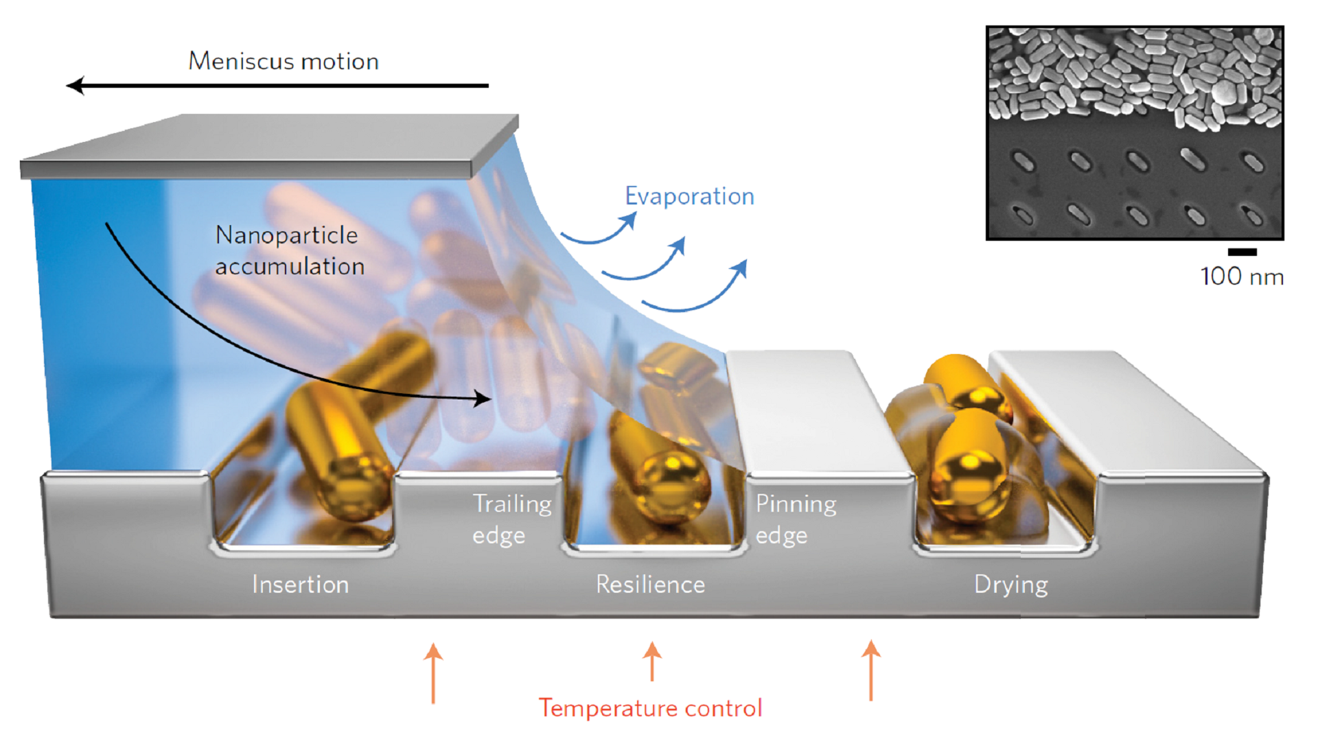
Predetermined and selective placement of nanoparticles onto large-area substrates with nanometre-scale precision is essential to harness the unique properties of nanoparticle assemblies, in particular for functional optical and electrooptical nanodevices. Unfortunately, such high spatial organization is currently beyond the reach of top-down nanofabrication techniques alone. Here, we demonstrate that topographic features comprising lithographed funnelled traps and auxiliary sidewalls on a solid substrate can deterministically direct the capillary assembly of Au nanorods to attain simultaneous control of position, orientation and interparticle distance at the nanometre level. We report up to 100% assembly yield over centimetre-scale substrates. We achieve this by optimizing the three sequential stages of capillary nanoparticle assembly: insertion of nanorods into the traps, resilience against the receding suspension front and drying of the residual solvent. Finally, using electron energy-loss spectroscopy we characterize the spectral response and near-field properties of spatially programmable Au nanorod dimers, highlighting the opportunities for precise tunability of the plasmonic modes in larger assemblies.
Self-assembly

Our work on nanoscale assembly:
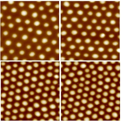
We demonstrate the controlled tuning of the characteristic dimensions of two-dimensional arrays of block-copolymer micelles. The arrays are obtained by spin-coating a solution of PS-b-P2VP (polystyrene-block-poly(2-vinylpyridine) micelles. The array periodicity, for example, can be systematically varied by changing the polymer concentration, the solvent composition, or the spin-coating parameters. The whole process is 4″ wafer compatible.
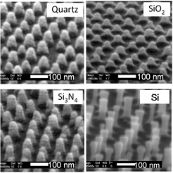
Block copolymer micelle lithography has been used to create nanopillars of tunable dimensions and different densities. Nanopillar arrays have been fabricated on different substrates such as silicon, silicon dioxide, silicon nitride and quartz. In this way, different functional surfaces and membranes have been fabricated, e.g. super-hydrophobic surfaces and nanoporous polymeric membranes and controlling the areal density of physical vapor deposition derived titanium nitride nanostructures.
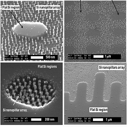
Combining block copolymer micelle lithography with stencil lithography is an excellent example for the combination of top-down with bottom-up fabrication methods. It offers a simple and cost-efficient means for the patterning of nanostructured surfaces. The stencil patterning can be done on the micron- and on the nano-scale. Complementary micro-/nanoarchitectures could thus be fabricated. The use of stencil lithography for the patterning of the nanoscale structures has several advantages over photoresist based patterning, particularly for the integration of nanostructures into on-chip device architectures.
Self-assembled polystyrene nanospheres are deposited on 4″ substrates by spin-coating. An initial template of wafer-scale monolayers of hexagonally close-packed beads can thus be realized. The dot array template can then be transferred into either dot or hole arrays in silicon based materials or metals. High aspect ratio silicon nanopillars, nanoporous SiN membranes and nanoporous thin metal films have been fabricated. The applications of such structures range from functional surfaces, filtration membranes or membranes for cell growth, over structures for optical effects to plasmonics.

Our work on microscale assembly:

Self-assembly of micro-components allows us to assemble huge number of micro-objects in scalable and parallel manner where the standard pick-and-place approach is fastidious. We demonstrate self-assembly of simple bicolor SU-8 cylinders as well as half capsules for liquid encapsulation and release. To ensure a successful encapsulation, face-selective surface functionalization has to be done by a silane “lift-off-like” process resulting in only one surface selectively more hydrophobic than all other ones. The half-capsules could be self-assembled in aqueous solutions into complete capsules encapsulating the solution with a yield above 95%, which could also be subsequently released in another medium.

We demonstrate self-assembly of microstructures by magnetic force. Microstrucutres of a superparamagnetic composite have been fabricated by inkjet printing. The structures have been made such that they involve magnetic easy axis. Bringing the structures in a fluidic phase allows to control them by an external magnetic field, allowing their self-organization and self-assembly. As a demonstrated their attraction and repulsion is shown as well as their self-organization into lines.
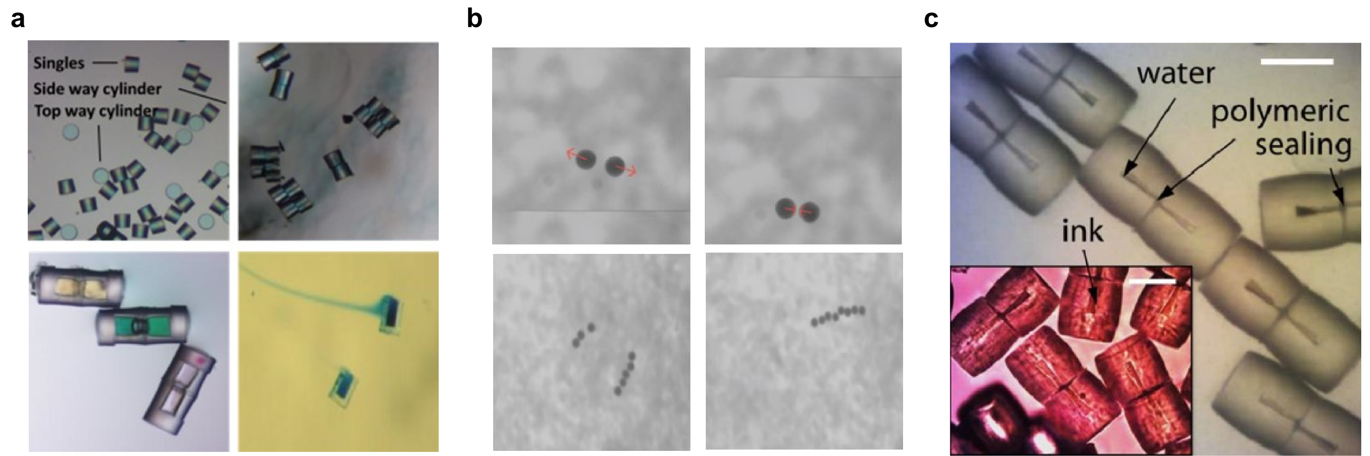
100 um half-capsules are fabricated by photolithography based on a prefabricated silicon substrate. The half-capsules are made hydrophilic except one surface kept hydrophobic. This allows in a fluidic phase to selectively precipitate a polymer solution – acting as a UV-glue – onto the surfaces of the half-capsules which will self-assemble into complete capsules. This leads us to sealed microcapsules encapsulating surrounding media. As a proof of concept, colored ink as been encapsulated.

Keywords: assembly, self-assembly


Journal papers


Comparison of electrical and optical transduction modes of DNA-wrapped SWCNT nanosensors for the reversible detection of neurotransmitters.

P. Clement; J. Ackermann; N. Sahin-Solmaz; S. Herbertz; G. Boero et al. 

Biosensors & Bioelectronics. 2022. Vol. 216, p. 114642. DOI : 10.1016/j.bios.2022.114642.

Precise Capillary‐Assisted Nanoparticle Assembly in Reusable Templates

H. Yu; A. Conde Rubio; H-C. Wang; O. Martin; G. Boero et al. 

Particle & Particle Systems Characterization. 2022.  p. 1 – 8, 2100288. DOI : 10.1002/ppsc.202100288.

Precision Surface Microtopography Regulates Cell Fate via Changes to Actomyosin Contractility and Nuclear Architecture

J. Carthew; H. H. Abdelmaksoud; M. Hodgson-Garms; S. Aslanoglou; S. Ghavamian et al. 

Advanced Science. 2021. Vol. 8, num. 6, p. 2003186. DOI : 10.1002/advs.202003186.

Electrochemical performance of polymer-derived SiOC and SiTiOC ceramic electrodes for artificial cardiac pacemaker applications

J. Jang; P. V. Warriam Sasikumar; F. Navaee; L. Hagelüken; G. Blugan et al. 

Ceramics International. 2020. Vol. 47, num. 6, p. 7593 – 7601. DOI : 10.1016/j.ceramint.2020.11.098.

Designs and Characterization of Subunit Ebola GP Vaccine Candidates: Implications for Immunogenicity

V. Agnolon; D. Kiseljak; M. J. Wurm; F. M. Wurm; C. Foissard et al. 

Frontiers In Immunology. 2020. Vol. 11, p. 586595. DOI : 10.3389/fimmu.2020.586595.

A 3D Microscaffold Cochlear Electrode Array for Steroid Elution

J. Jang; J. Kim; Y. C. Kim; S. Kim; N. Chou et al. 

Advanced Healthcare Materials. 2019.  p. 1900379. DOI : 10.1002/adhm.201900379.

Liquid Assembly of Floating Nanomaterial Sheets for Transparent Electronics

Z. Su; H. S. C. Yu; X. Zhang; J. Brugger; H. Zhang 

Advanced Materials Technologies. 2019.  p. 1900398. DOI : 10.1002/admt.201900398.

Combination of thermal scanning probe lithography and ion etching to fabricate 3D silicon nanopatterns with extremely smooth surface

Y. Lisunova; J. Brugger 

Microelectronic Engineering. 2018. Vol. 193, p. 23 – 27. DOI : 10.1016/j.mee.2018.02.012.

3D printed microchannels for sub-nL NMR spectroscopy

E. Montinaro; M. Grisi; M. C. Letizia; L. Pethö; M. A. M. Gijs et al. 

PLOS ONE. 2018. Vol. 13, num. 5, p. e0192780. DOI : 10.1371/journal.pone.0192780.

Optical Antenna-Based Fluorescence Correlation Spectroscopy to Probe the Nanoscale Dynamics of Biological Membranes

P. Winkler; R. Regmi; V. Flauraud; J. Brugger; H. Rigneault et al. 

The Journal of Physical Chemistry Letters. 2018. num. 9, p. 110 – 119. DOI : 10.1021/acs.jpclett.7b02818.

NMR spectroscopy of single sub-nL ova with inductive ultra-compact single-chip probes

M. Grisi; F. Vincent; B. Volpe; R. Guidetti; N. Harris et al. 

Scientific Reports. 2017. Vol. 7, p. 44670. DOI : 10.1038/srep44670.

Nanopatterning of a Stimuli-Responsive Fluorescent Supramolecular Polymer by Thermal Scanning Probe Lithography

S. T. Zimmermann; D. W. H. Balkenende; A. Lavrenova; C. Weder; J. Brugger 

ACS Applied Materials and Interfaces. 2017. Vol. 9, num. 47, p. 41454 – 41461. DOI : 10.1021/acsami.7b13672.

Growth Of Organic Semiconductor Thin Films with Multi-Micron Domain Size and Fabrication of Organic Transistors Using a Stencil Nanosieve

P. Fesenko; V. Flauraud; S. Xie; E. Kang; T. Uemura et al. 

ACS Applied Materials & Interfaces. 2017. Vol. 9, num. 28, p. 23314 – 23318. DOI : 10.1021/acsami.7b06584.

Silicon nanostructures for bright field full color prints

V. Flauraud; M. Reyes; R. Paniagua-Dominguez; A. Kuznetsov; J. Brugger 

ACS Photonics. 2017. Vol. 4, num. 8, p. 1913 – 1919. DOI : 10.1021/acsphotonics.6b01021.

High sensitivity field asymmetric ion mobility spectrometer

M. A. Chavarria; A. V. Matheoud; P. Marmillod; Y. Liu; D. Kong et al. 

Review of Scientific Instruments. 2017. Vol. 88, num. 3, p. 035115 – 1. DOI : 10.1063/1.4978960.

High-aspect ratio nanopatterning via combined thermal scanning probe lithography and dry etching

Y. Lisunova; M. Spieser; R. Juttin; F. Holzner; J. Brugger 

Microelectronic Engineering. 2017. Vol. 180, p. 20 – 24. DOI : 10.1016/j.mee.2017.04.006.

Planar Optical Nanoantennas Resolve Cholesterol-Dependent Nanoscale Heterogeneities in the Plasma Membrane of Living Cells

R. Regmi; P. M. Winkler; V. Flauraud; K. J. E. Borgman; C. Manzo et al. 

Nano Letters. 2017. Vol. 17, num. 10, p. 6295 – 6302. DOI : 10.1021/acs.nanolett.7b02973.

Mode Evolution in Strongly Coupled Plasmonic Dolmens Fabricated by Templated Assembly

V. Flauraud; G. D. Bernasconi; J. Butet; M. Mastrangeli; D. T. L. Alexander et al. 

ACS Photonics. 2017. Vol. 4, num. 7, p. 1661 – 1668. DOI : 10.1021/acsphotonics.6b01026.

Nanoscale topographical control of capillary assembly of nanoparticles

V. Flauraud; M. Mastrangeli; G. D. Bernasconi; J. Butet; D. T. L. Alexander et al. 

Nature Nanotechnology. 2017. Vol. 12, num. 1, p. 73 – 80. DOI : 10.1038/nnano.2016.179.

Transient Nanoscopic Phase Separation in Biological Lipid Membranes Resolved by Planar Plasmonic Antennas

P. M. Winkler; R. Regmi; V. Flauraud; J. Brugger; H. Rigneault et al. 

ACS Nano. 2017. Vol. 11, num. 7, p. 7241 – 7250. DOI : 10.1021/acsnano.7b03177.

Conference papers


Harnessing Poisson Effect to Realize Tunable Tunneling Nanogap Electrodes on PDMS Substrates for Strain Sensing

H. S. Yu; G. Boero; J. Brugger 

2019. 20th International Conference on Solid-State Sensors, Actuators and Microsystems & Eurosensors XXXIII (TRANSDUCERS & EUROSENSORS XXXIII), Berlin, Germany, June 23-27, 2019. p. 2368 – 2371. DOI : 10.1109/TRANSDUCERS.2019.8808819.

Self-assembly of micro/nanosystems across scales and interfaces

M. Mastrangeli 

2017. 19th International Conference on Solid-State Sensors, Actuators and Microsystems (TRANSDUCERS 2017), Kaohsiung, Taiwan, June 18-22, 2017. p. 676 – 681. DOI : 10.1109/TRANSDUCERS.2017.7994139.

Shift Dynamics of Capillary Self-Alignment

G. Arutinov; M. Mastrangeli; E. C. P. Smits; G. van Heck; H. F. M. Schoo et al. 

2014. International Precision Assembly Seminar (IPAS 2014), Chamonix, FR, February 16-18, 2014. p. 61 – 68. DOI : 10.1007/978-3-662-45586-9_9.

Automated Real-Time Control of Fluidic Self-Assembly of Microparticles

M. Mastrangeli; F. S. Schill; J. Goldowsky; H. Knapp; J. Brugger et al. 

2014. 2014 IEEE International Conference on Robotics and Automation (ICRA 2014), Hong Kong (China), May 31 – June 7, 2014. p. 5860 – 5865. DOI : 10.1109/ICRA.2014.6907721.

Liquid-Filled Sealed Mems Capsules Fabricated By Fluidic Self-Assembly

M. Mastrangeli; L. Jacot-Descombes; M. R. Gullo; J. Brugger 

2014. IEEE International Conference on Micro Electro Mechanical Systems (MEMS 2014), San Francisco (USA), January 26-30, 2014. p. 56 – 59. DOI : 10.1109/MEMSYS.2014.6765572.

In-liquid MEMS assembly by optical trapping

M. R. Gullo; L. Jacot-Descombes; J. Brugger 

2013. 2013 IEEE 26th International Conference on Micro Electro Mechanical Systems (MEMS), Taipei, Taiwan, 20-24 01 2013. p. 78 – 81. DOI : 10.1109/MEMSYS.2013.6474181.

Polymeric hemispherical pico-liter micro cups fabricated by inkjet printing

L. Jacot-Descombes; M. R. Gullo; V. J. Cadarso; M. Mastrangeli; J. Brugger 

2013. 2013 8th IEEE International Conference on Nano/Micro Engineered and Molecular Systems (NEMS), Suzhou, China, 7-10 04 2013. p. 1119 – 1122. DOI : 10.1109/NEMS.2013.6559918.

Stencil-nanopatterned back reflectors for thin-film amorphous silicon n-i-p solar cells

C. Pahud; V. Savu; M. Klein; O. Vazquez-Mena; K. Soederstroem et al. 

2012. 38th IEEE Photovoltaic Specialists Conference (PVSC). p. 694 – 696. DOI : 10.1109/PVSC.2012.6317704.

Characterization of Hydrophobic Forces for in Liquid Self-Assembly of Micron-Sized Functional Building Blocks

R. M. Gullo; L. Jacot-Descombes; L. Aeschimann; J. Brugger 

2011. 2010 MRS Fall Meeting, Boston, Massachusetts, USA, November 30-December 2, 2010. DOI : 10.1557/opl.2011.466.

Sub-100 nm-scale Aluminum Nanowires by Stencil Lithography: Fabrication and Characterization

O. Vazquez-Mena; V. Savu; K. Sidler; G. Villanueva; M. A. F. van den Boogaart et al. 

2008. 3rd IEEE International Conference of Nano/Micro Engineered and Molecular Systems, Sanya, Hainan Island, China, January 6-9, 2008.. p. 807 – 811. DOI : 10.1109/NEMS.2008.4484447.

Discontinuous Palladium Nanostructures for H2 Sensing

C. Fournier; T. Kiefer; L. G. Villanueva; F. Fargier; J. Brugger et al. 

2008. ECS Transactions, Hawaii, 2008. p. 457 – 463. DOI : 10.1149/1.2981151.