| Group members | N. Wyrsch, Y. Riesen, S. Dunand |
| Running projects: | SNFS project, EOS Holding, CTI project, OFEN-EWG, SCCER Furies and external mandates |
Keywords: Particle sensors, imagers, thin-film transistors, energy storage, energy scavenging, functional coatings
Background and research interest
Using the know-how and expertise of the laboratory, the developed materials and methods can be applied to other applications. The thin-film electronics groups is focusing mainly on the development of sensors, imagers and energy scavengers, but is also active in PV system aspects such as the local storage of PV electricity.
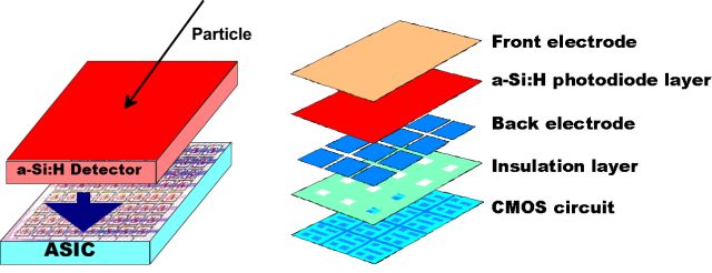
Thin-film silicon based solar cells have the advantage to be compatible with many types of substrates, such as rigid or flexible, transparent or opaque substrates. Such devices can be used as light or particle sensors and monolithically integrated in complicated devices or microsystems. For example, array of sensor diodes can be realized by depositing amorphous silicon directly on top of pixelized readout electronics (so called TFA – Thin Film on ASIC or TFC – Thin Film on CMOS technology, see Fig. 1) or embedded in microfluidics systems. In the context of particle detection, amorphous silicon (a-Si:H) based sensors are also very attractive given the high radiation hardness of the material.
|
|
|
| Figure 1. Concept of thin-film on ASIC (TFA) particle detector (left) and schematic view of its components (right). | |
a-Si:H based layers can also be used in other type of devices such as thin-film transistors, optical components or used as functional coatings. The expertise of the laboratory is used here for providing coatings of thickness up to 100 µm on various substrates with various morphologies.
With a relatively large and tunable bandgap, a-Si:H based solar cells are ideally adapted for energy scavenging for indoor applications. The possibility of processing it on various substrates, the opportunity of a monolithic integration and the flexibility in the design of solar modules with suitable electrical output make this technology very attractive for various applications (indoor but also outdoor) where a local source of energy is desirables.
Growing share of electricity generated from intermittent renewable energy sources, including from photovoltaic (PV) systems, calls for storage solutions. Decentralized storage solutions are also expected to ease the growing integration of PV systems in electrical networks. For this purpose, PV systems comprising a battery storage are an attractive option. Design of such a system and energy storage strategy (in relation with the PV part) are here of great interests. Knowledge on the energy yield of such system, including of all components is required, including of the solar cells.
A better understanding and modelling of the energy yield of the cell should also permit an optimization of the device for maximum energy production rather than for maximum efficiency. Such a change of paradigm should be helpful for both consumers and producers of solar cells and modules.
Research highlights
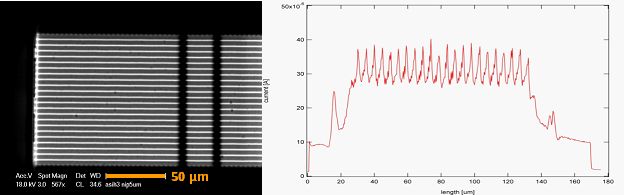
In the last years several types of TFA detectors have been developed as imager, or pixelized particle detectors for the detection of beta, protons, or X-ray particles. Such detectors can exhibit very high spatial resolutions (better than 3 microns – for 1D and 2D configurations) as demonstrated from test structures using microstrip design (see Fig. 2).
 |
|
| Figure 2. Electron beam induced current (EBIC) map (left) as well as EBIC linear scan on a series of 1.5 µm wide microstrips spaced by 3.5 µm and covered with a 5 µm thick a-Si:H n-i-p diode. Picture published by N. Wyrsch in the MRS Proc. Vol. 1321 (2012) 423-434 |
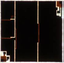
Microchannel plates (MCP) are electron multiplication devices used in image intensifiers, as well as for specific applications in high energy physics, astrophysics, biology and medicine. They consist in thick (about half of a millimeter) glass plates with micrometer-wide channels throughout the plate. The channel length-over-diameter aspect ratio is between 40:1 and 60:1. When an electron hits the channel surface, it produces the emission of a few secondary electrons, which are accelerated by the high electric field applied across the plate. This effect leads to more collisions along the channel and to a multiplication (or avalanche) of electrons (Fig. 3 left), similarly to photomultiplier tubes with discrete dynodes. Recently, CERN and our lab proposed to use a-Si:H instead of glass to fabricate MCP. a-Si:H exhibits ideal material and electrical properties for such application, it can be micro-machined with standard crystalline silicon techniques to drill the microchannels and it can be deposited on the readout electronics to realize monolithic devices (Fig. 3 left). After the realization of first prototypes and demonstration of multiplication of electrons in a-Si:H microchannels, the MCP design was radically modified with the implementation of an additional intermediate electrode, made of n-doped microcrystalline silicon layer (<n> uc-Si:H). As shown in Fig. 3 right, this electrode evacuates the leakage current, which flows through the AMCP bulk due to the large applied bias voltage, while the multiplied electrons are collected by the bottom electrodes (anodes). This reduces by several orders of magnitude the influence of leakage on the signal output and the sensitivity to the electron multiplication signal is enhanced. With this improved structure we were able to quantify the multiplication gain for a number of AMCP with various geometrical features. A a maximum gain of 110 was measured for an aspect ratio of 12:1 and an accelerating electric field of 7∙104 V/cm. More details, can be found in Ref [1].
|
|
|
| Figure 3. a-Si:H based MCP structure (left) and SEM micrograph of cross-section of a fabricated device (right). | |

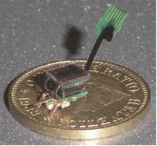
In the framework of a EU project (I-Swarm) autonomous microrobots were developed. EPFL PV-Lab was in charge of the development of the PV module needed for powering the robot. This module comprises several diode segments delivering 1.5 and 3.3 V as well as 2 photodiodes (Fig. 4). For this kind of applications, a-Si:H technology offers several key advantages: flexibility in designing the PV modules (shape, substrate materials), and the electrical characteristics of the module, high performance under artificial light. While the efficiency of a-Si:H solar cells can reached 10% under sun illumination, the efficiency easily exceeds 20% under artificial light in indoor conditions (fluorescent light spectrum at 1000 Lux).
 |
 |
 |
| Figure 4: Top top view of a solar module (center) developed for an autonomous micro-robot with a size of 4x4x4 mm3 (left). A schematic design of the solar module is given on the right picture. | ||
Outlook
Within the next years, the group will investigate the different topics mentioned above more in details. The focus will be put on
• Further development of particle sensors in TFA technology, especially for high irradiation conditions
• Demonstration of a-Si:H based MCP as a viable alternative to glass based MCP
• Development of very efficient PV devices for low intensity indoor illumination
• Models for the energy yield determination of PV cells and modules and especially of multi-junction thin-film silicon ones
• PV electricity storage strategies and solutions to ease the penetration of PV in the electrical networks.
Key publications
| [1] | A. Franco, J. Geissbühler, N. Wyrsch, C. Ballif, Fabrication and characterization of monolithically integrated microchannel plates based on amorphous silicon, Scientific Reports 4, Article number: 4597, doi:10.1038/srep04597 |
| [2] | A. Franco, Y. Riesen, M. Despeisse, N. Wyrsch, C. Ballif, High Spatial Resolution of Thin-Film-on-ASIC Particle Detectors, IEEE Trans. on Nucl. Sc. 59 (2012) 2614-2621, http://dx.doi.org/10.1109/TNS.2012.2208478 |
| [3] | N. Wyrsch, A. Franco, Y. Riesen, M. Despeisse, S. Dunand, F. Powolny, P. Jarron, C. Ballif, Amorphous Silicon Based Particle Detectors, MRS Symp. Proc. Vol. 1321 (2012) 423-434 |
| [4] | A. Franco, Y. Riesen, N. Wyrsch, S. Dunand, F. Powolny, P. Jarron, C. Ballif, Amorphous silicon-based microchannel plates, http://dx.doi.org/10.1016/j.nima.2011.11.089 |
| [5] | M. Moridi, S. Tanner, N. Wyrsch, P.A. Farine, S. Rohr, An amorphous silicon photodiode array for glass-based optical MEMS application, IEEE SENSORS 2009 (2009) 1604 – 1608 http://dx.doi.org/10.1109/ICSENS.2009.5398496 |
| [6] | Y. Bilevych, V.M. Blanco Carballo, M. Chefdeville, P. Colas, E. Delagnes, M. Fransen, H. vander Graaf, W.J.C. Koppert, J. Melai, C. Salm, J.Schmitz, J. Timmermans, N. Wyrsch, Spark protection layers for CMOS pixel anode chips in MPGDs, Nucl. Instr. and Meth. In Phys, Res. A 629 (2011) 66–73 |
| [7] | G. Choong, N. Wyrsch, M. Python C. Ballif, High mobility bottom gate microcrystalline silicon TFT deposited by VHF PECVD, Proc. of the International Thin Film Transistor Conference ITC’09, Palaiseau, France, (2009) 43-46 |
| [8] | N. Wyrsch, S. Dunand, C. Ballif. Micro Photovoltaic Modules for Micro Systems, MRS Symp. Proc. Vol. 1066 (2008) A10-4 |