January/February 2025

This image showcases a nanoprinted miniature of EPFL’s iconic Rolex Learning Center, fabricated at CMI. The structure was created using two-photon lithography (Nanoscribe) to pattern a polymer template, followed by atomic layer deposition (ALD) to coat it with nickel (Ni), replicating the architectural curves with nanoscale precision. This work exemplifies the power of advanced nanofabrication techniques, merging architectural beauty with cutting-edge material science. Microscope: SEM Merlin. 1/13

A beautifully shaped zeolite crystal which resembles a wooden road signboard. Microscope: SEM Teneo. 2/13

Get shrunk and get in. Except the oversized ones, everyone is welcome. The terrain is nonconductive, but don’t worry, the drive will conduct well the train, even in 75 (45+30) degree slopes … Microscope: SEM Merlin. 3/13

Small chalcogenide glass fragments suspending on the polymer substrate look like tiny mineral grown in the cave. Microscope: SEM Gemini. 4/13

While investigating my samples, I stumbled upon this area that looks like some micro-spiders have build their nest and deposited some eggs here. Microscope: SEM Gemini. 5/13

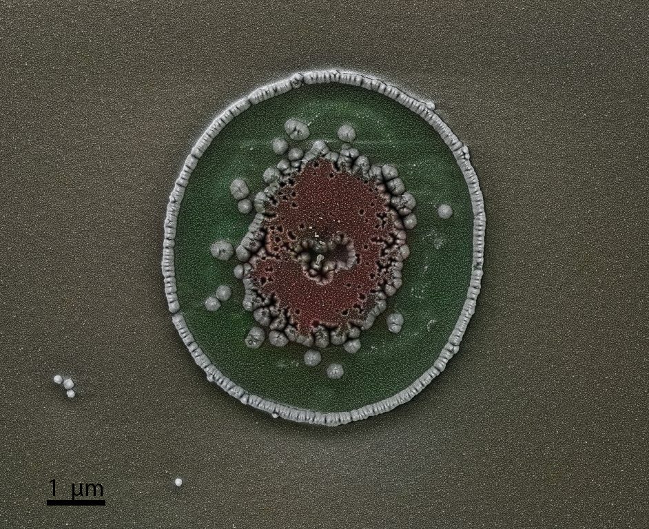
While thinking about summer vacation, I stumbled upon this section of my sample, that reminded me of a coral reef. Maybe this will help fight the winter blues until we see more sun! Microscope: SEM Gemini. 6/13

Sometimes, while exploring the unknown, one might stumble upon caves filles with precious glowstones. Be quick to pick them up for your future journey. Microscope: SEM Gemini. 7/13

FIB cross-section of a 160 nm VO2 nanowire and 60 nm VO2 bottom layer on top of a Si chip with 200 nm SiO2 and covered with 20 nm Cr and 150 nm Au contact. The nanowire has been obtained by ion beam etching (IBE) with Ar, using 900 nm HSQ (e-beam lithography resist) as a mask. The combination of the high aspect ratio, the typical IBE redeposition, and the -10° angle and rotation during the etching has produced the antenna-like VO2 structures. The chip was fabricated by Vanessa Conti and Andrea Iaconeta in CMi, the FIB lamella and TEM analysis have been done by me. The space invader aliens have been added in post-production. Microscope: TEM Talos. 8/13

A defect in a cured transparent resist created wrinkles, forming wave-like structures. During the dewetting of a thin selenium film, droplets formed and settled on the surface, appearing to float on the waves. Microscope: SEM Gemini. 9/13

An SEM image of coffin-shaped zeolite crystals. Microscope: SEM Teneo. 10/13

Some zeolite crystals deposited on graphite closely resemble a bunch of coffins. Microscope: SEM Teneo. 11/13

A heart-shaped structure intricately designed from covalent organic framework nanotubes, resembling a blooming flower—an elegant fusion of porosity and precision that breathes life into material science. Microscope: SEM Teneo. 12/13
nP grown my MBE turns contamination into fascinating art – shaping intricate, fortress-like layers that echo medieval defenses. Microscope: SEM Merlin. 13/13

This image showcases a nanoprinted miniature of EPFL’s iconic Rolex Learning Center, fabricated at CMI. The structure was created using two-photon lithography (Nanoscribe) to pattern a polymer template, followed by atomic layer deposition (ALD) to coat it with nickel (Ni), replicating the architectural curves with nanoscale precision. This work exemplifies the power of advanced nanofabrication techniques, merging architectural beauty with cutting-edge material science. Microscope: SEM Merlin.

A beautifully shaped zeolite crystal which resembles a wooden road signboard. Microscope: SEM Teneo.

Get shrunk and get in. Except the oversized ones, everyone is welcome. The terrain is nonconductive, but don’t worry, the drive will conduct well the train, even in 75 (45+30) degree slopes … Microscope: SEM Merlin.

Small chalcogenide glass fragments suspending on the polymer substrate look like tiny mineral grown in the cave. Microscope: SEM Gemini.

While investigating my samples, I stumbled upon this area that looks like some micro-spiders have build their nest and deposited some eggs here. Microscope: SEM Gemini.

While thinking about summer vacation, I stumbled upon this section of my sample, that reminded me of a coral reef. Maybe this will help fight the winter blues until we see more sun! Microscope: SEM Gemini.

Sometimes, while exploring the unknown, one might stumble upon caves filles with precious glowstones. Be quick to pick them up for your future journey. Microscope: SEM Gemini.

FIB cross-section of a 160 nm VO2 nanowire and 60 nm VO2 bottom layer on top of a Si chip with 200 nm SiO2 and covered with 20 nm Cr and 150 nm Au contact. The nanowire has been obtained by ion beam etching (IBE) with Ar, using 900 nm HSQ (e-beam lithography resist) as a mask. The combination of the high aspect ratio, the typical IBE redeposition, and the -10° angle and rotation during the etching has produced the antenna-like VO2 structures. The chip was fabricated by Vanessa Conti and Andrea Iaconeta in CMi, the FIB lamella and TEM analysis have been done by me. The space invader aliens have been added in post-production. Microscope: TEM Talos.

A defect in a cured transparent resist created wrinkles, forming wave-like structures. During the dewetting of a thin selenium film, droplets formed and settled on the surface, appearing to float on the waves. Microscope: SEM Gemini.

An SEM image of coffin-shaped zeolite crystals. Microscope: SEM Teneo.

Some zeolite crystals deposited on graphite closely resemble a bunch of coffins. Microscope: SEM Teneo.

A heart-shaped structure intricately designed from covalent organic framework nanotubes, resembling a blooming flower—an elegant fusion of porosity and precision that breathes life into material science. Microscope: SEM Teneo.

nP grown my MBE turns contamination into fascinating art – shaping intricate, fortress-like layers that echo medieval defenses. Microscope: SEM Merlin.