November/December 2021 competitors
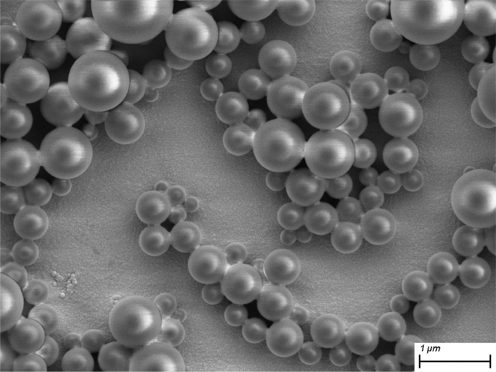
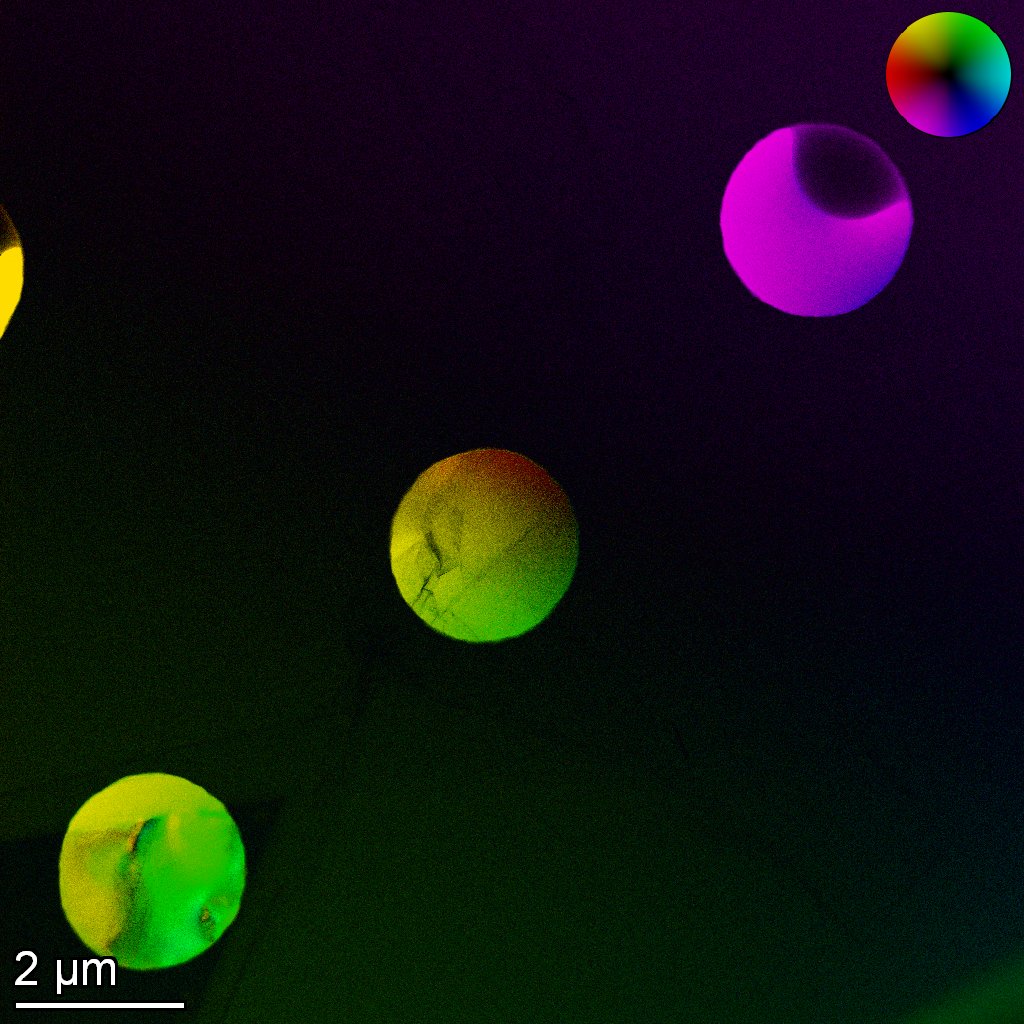
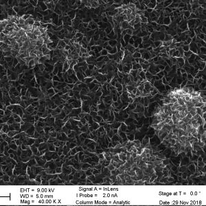
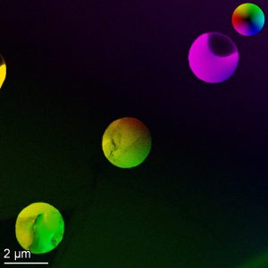
The spheres are self-assembled polymeric micelles, deposited on a conductive surface. Microscope: SEM Merlin 1/7
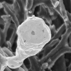
The beauty of nature looking at you. A mysterious compound containing mainly alkali at the surface of polished concrete immersed for 3 months in an alkaline solution. Microscope: SEM Merlin 2/7
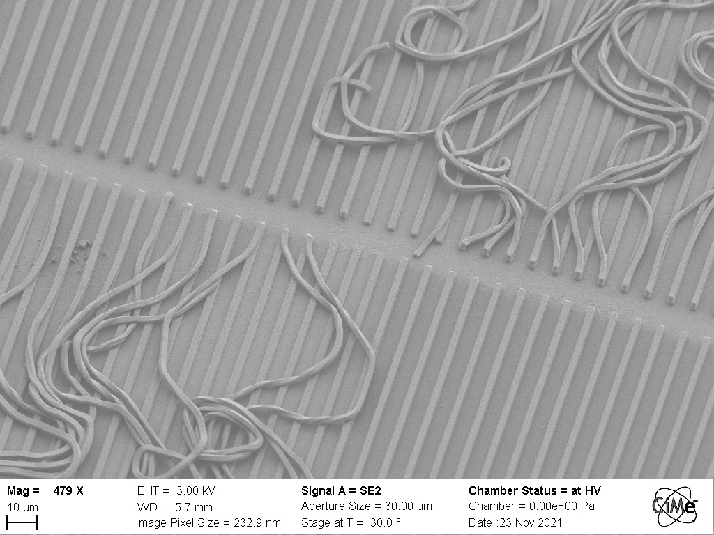
Beware, this micro-army of sneaky snakes is coming to life! A photolithographic resist pattern was used as a mask for dry etching a polymer. Incomplete stripping of the resist in acetone lead to lines still attached at their ends. Microscope: SEM Gemini 3/7
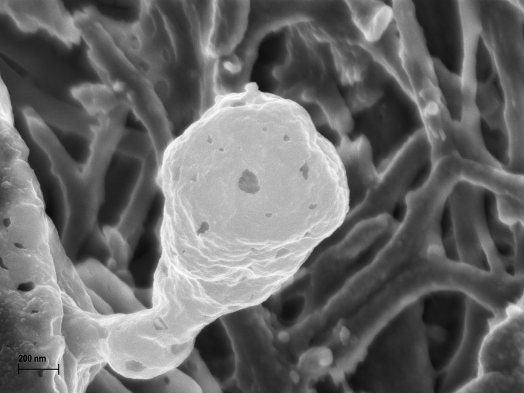
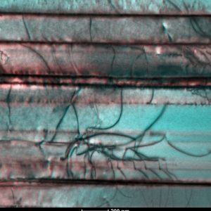
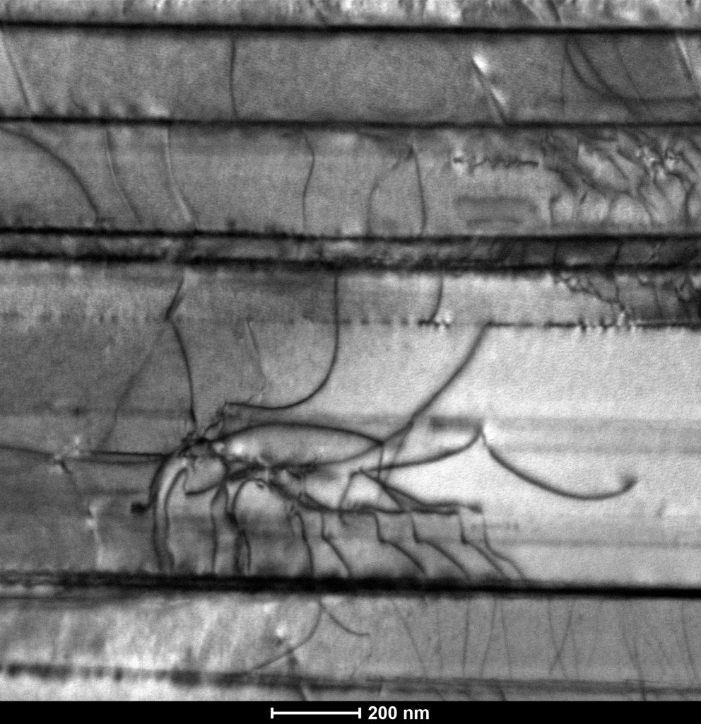
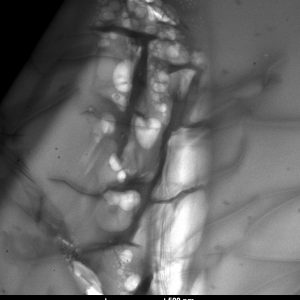
The Postsynaptic face of a dendritic spine Osmium coated rat nerve cell culture Photographed with SEM gemini Zeiss at 2kv scale bar on bottom left is 200nm. 4/7
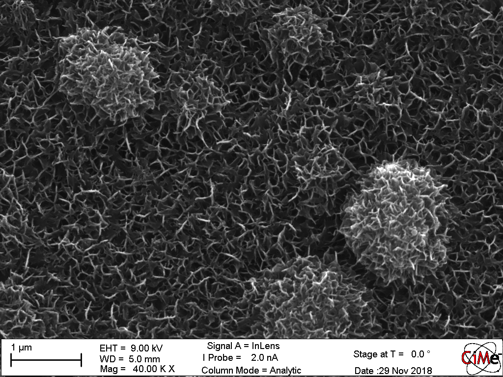
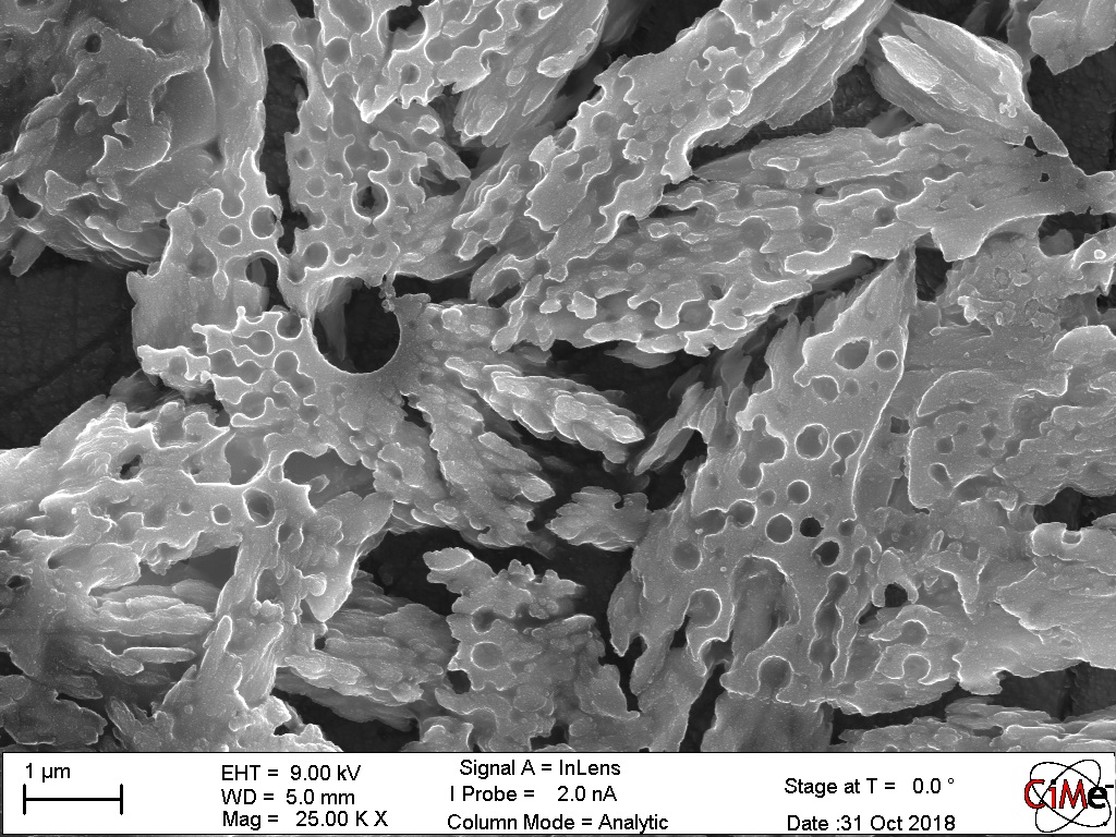
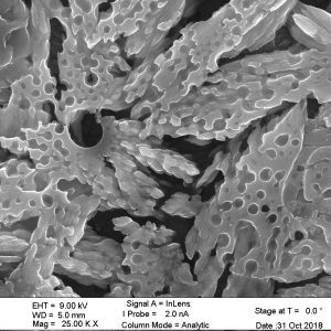
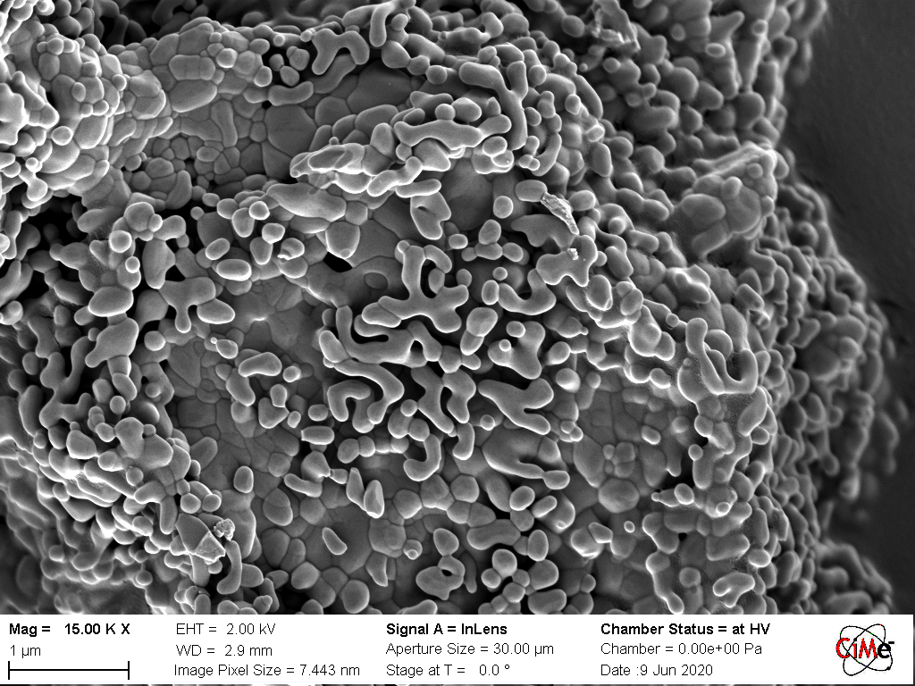
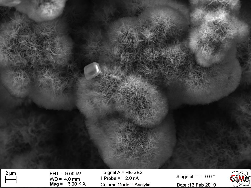
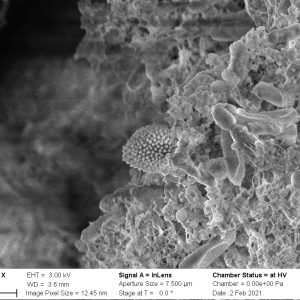
Silico-calco-potassium corals on the surface of concrete. Microscope: SEM Merlin 5/7
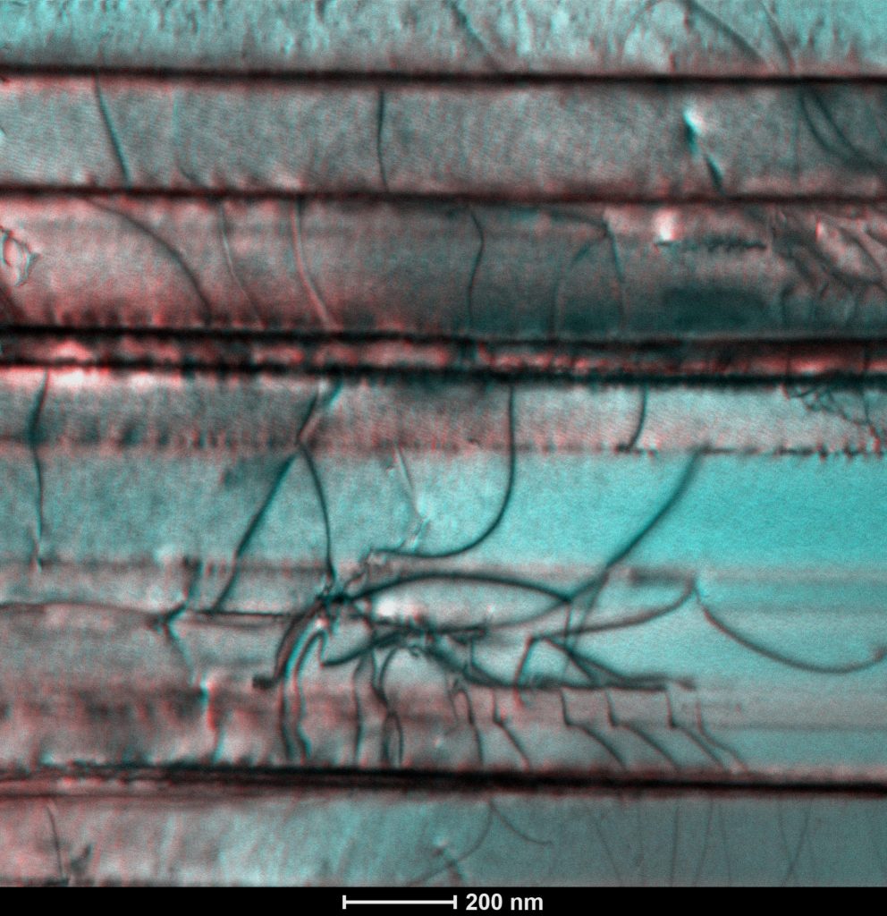
Differential phase contrast (DPC) imaging of freestanding 2D materials with thickness variations. Microscope: TEM Themis 6/7
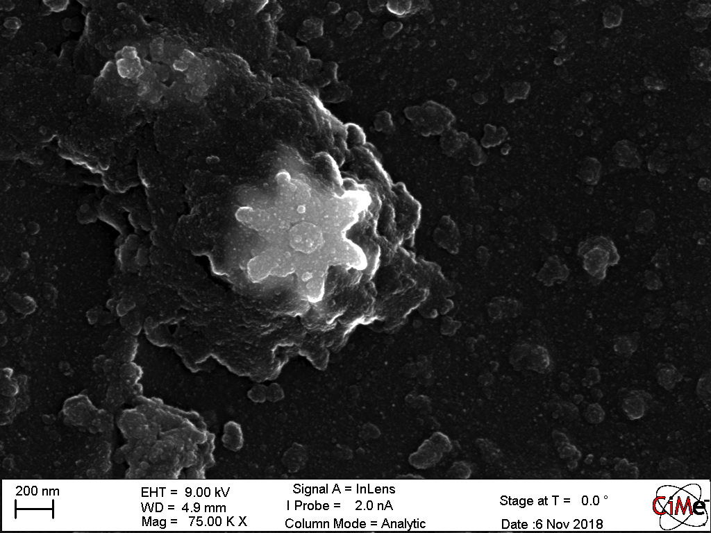
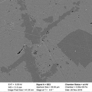
A beautiful star of unknown composition at the surface of concrete after 7 days of immersion in alkaline solution. Moral? Accumulate electrons to shine like a star. Microscope: SEM Merlin 7/7
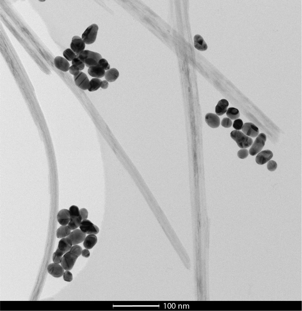
The spheres are self-assembled polymeric micelles, deposited on a conductive surface. Microscope: SEM Merlin
The beauty of nature looking at you. A mysterious compound containing mainly alkali at the surface of polished concrete immersed for 3 months in an alkaline solution. Microscope: SEM Merlin
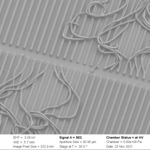
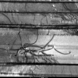
Beware, this micro-army of sneaky snakes is coming to life! A photolithographic resist pattern was used as a mask for dry etching a polymer. Incomplete stripping of the resist in acetone lead to lines still attached at their ends. Microscope: SEM Gemini
The Postsynaptic face of a dendritic spine Osmium coated rat nerve cell culture Photographed with SEM gemini Zeiss at 2kv scale bar on bottom left is 200nm.
Silico-calco-potassium corals on the surface of concrete. Microscope: SEM Merlin
Differential phase contrast (DPC) imaging of freestanding 2D materials with thickness variations. Microscope: TEM Themis
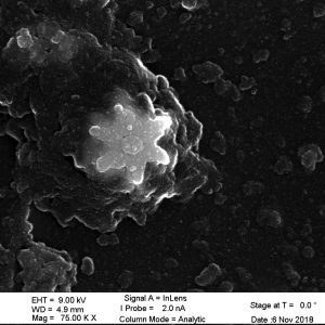
A beautiful star of unknown composition at the surface of concrete after 7 days of immersion in alkaline solution. Moral? Accumulate electrons to shine like a star. Microscope: SEM Merlin
September/October 2021 competitors
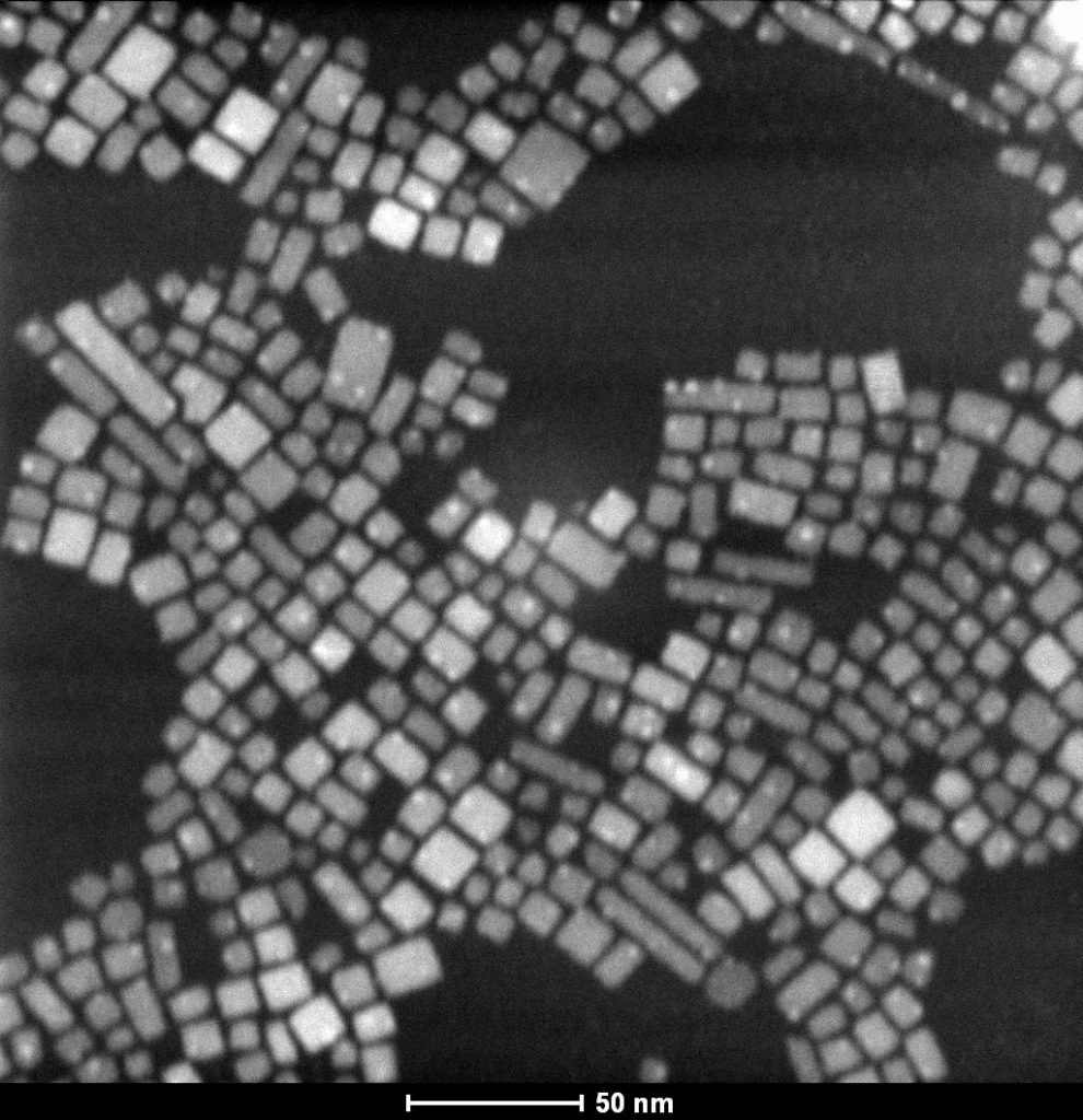
Perovskite nanocubes (and rectangles ..). All the merit goes to Colin Jeanguenat, I was just the TEM user 🙂 Microscope: TEM Osiris. 1/4
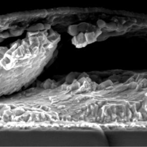
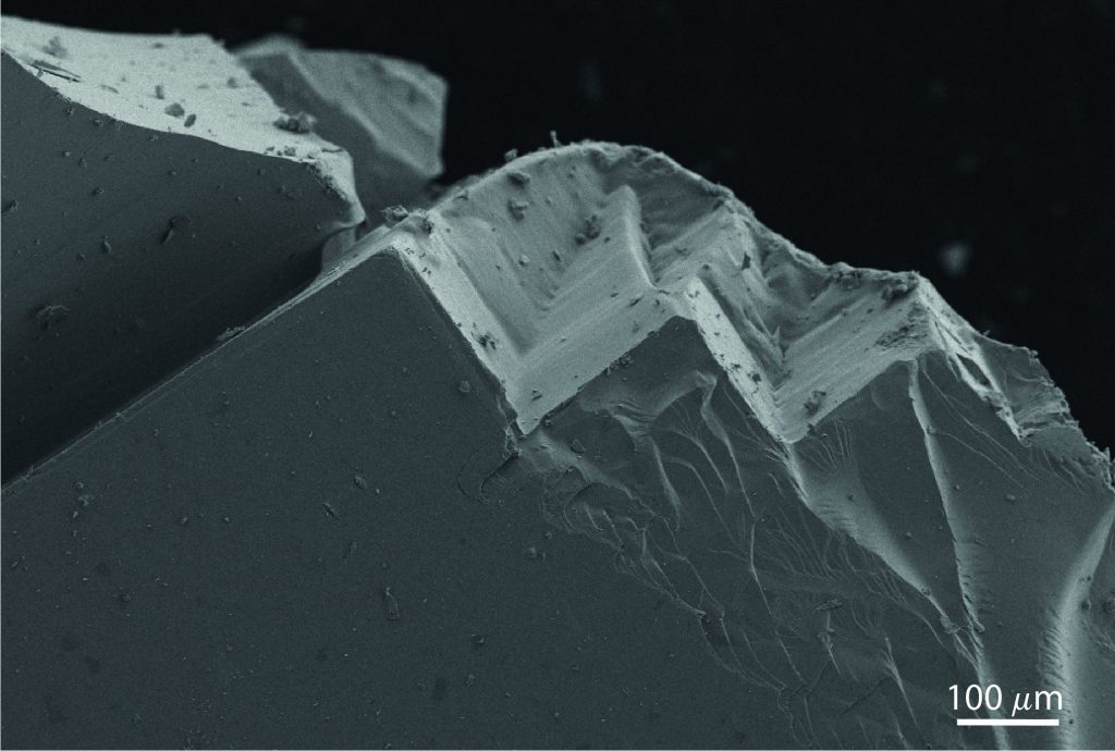
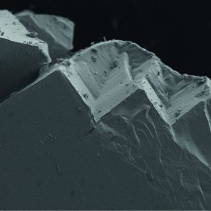
Cross-section of a thin film trampled by a monster cheese loaf and his gigantic shoe ! Microscope: SEM Gemini 2/4

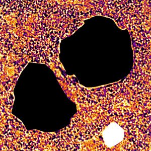
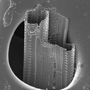
Assembly of gold nanoparticles on a ceramic nanofiber. Microscope: TEM Talos. 3/4
Anaglyph made from tilt-less stereo-pair STEM images of dislocations in TiAl alloy, stereo-angle approximately 2 degrees. Best viewed with 3D glasses. Microscope: TEM Osiris. 4/4
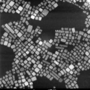
Perovskite nanocubes (and rectangles ..). All the merit goes to Colin Jeanguenat, I was just the TEM user 🙂 Microscope: TEM Osiris.
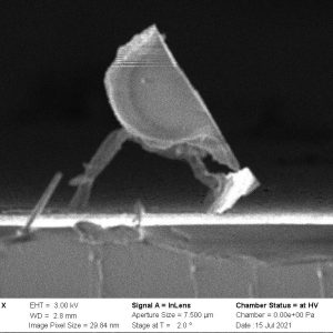
Cross-section of a thin film trampled by a monster cheese loaf and his gigantic shoe ! Microscope: SEM Gemini
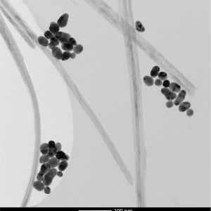
Assembly of gold nanoparticles on a ceramic nanofiber. Microscope: TEM Talos.
Anaglyph made from tilt-less stereo-pair STEM images of dislocations in TiAl alloy, stereo-angle approximately 2 degrees. Best viewed with 3D glasses. Microscope: TEM Osiris.
Do you want to participate? Read contest rules and submit your image(s) here.
May/June 2021 competitors
Bright-field image of dislocations in TiAl alloy acquired in two-beam diffraction condition. TEM Osiris. 1/9
This is a photo of a Metal-Organic Framework (MOF) crystalline superstructure synthesised by spray-drying method. The image has been acquired using FEI Teneo SEM in Sion. 2/9
Cutting out a filter contained in a single-use mask to keep us safe during the global coronavirus pandemic. SEM Merlin.
3/9
Pyrite (FeS2) particle surface after calcination at 800°C. During the process, pyrite decomposes releasing SO2 gas and transforms into iron oxide. The process sometimes involves some degree of melting, resulting in the liquid-like morphology observed here. Particle mounted in carbon film, coated with 4nm Ir. GeminiSEM 300. 4/9
Carboaluminate (AFm) precipitated in the shape of a surfer “riding” a grain of un-hydrated cement and surrounded by C-A-S-H. Polished section of LC3. SEM Merlin. 5/9
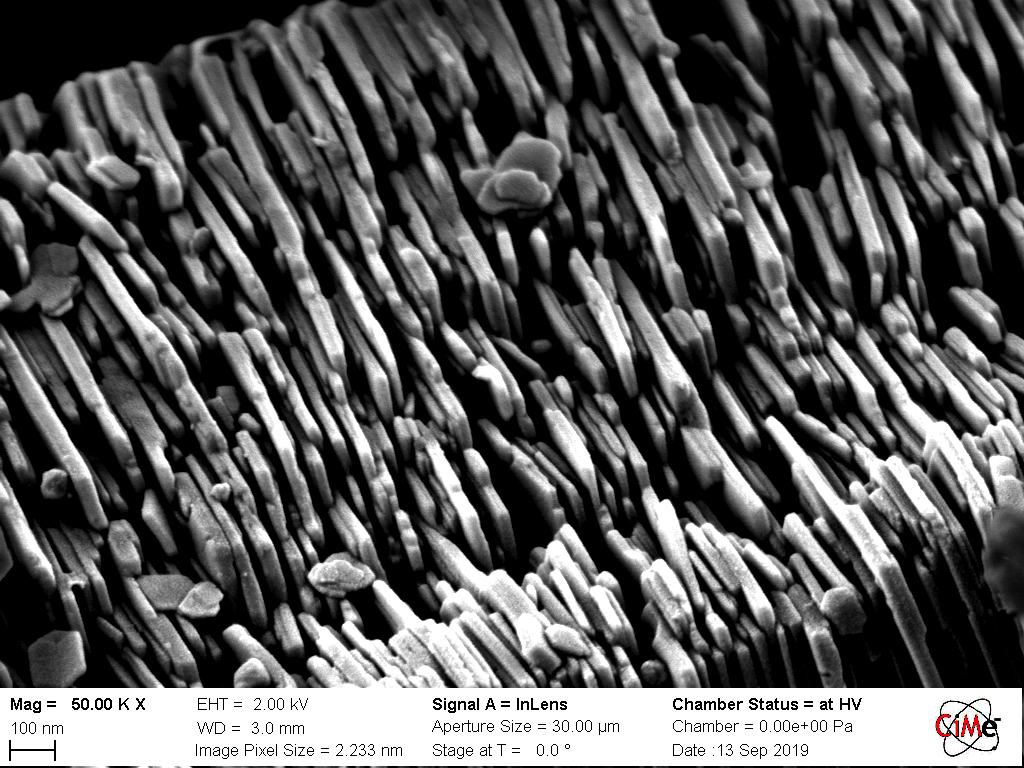
Kaolinite particle mounted over carbon film, coated with 4nm Ir, showing the multiple layers that form the clay’s particle structure and gives them their characteristic high surface area. GeminiSEM 300. 6/9
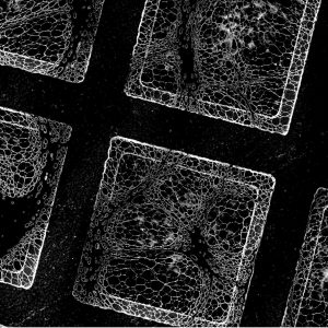
A failed yet beautiful attempt towards the optimization of poly(triazine imide) membranes. We deposited single-layer poly(triazine imide)nanosheets on a porous alumina support. Microscope: SEM Teneo.
7/9
Assembly of gold nanoparticles on a ceramic nanofiber. TEM Talos. 8/9
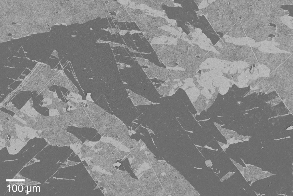
The image is from a polished surface of natural aggregate. GeminiSEM 300. 9/9
Bright-field image of dislocations in TiAl alloy acquired in two-beam diffraction condition. TEM Osiris.
This is a photo of a Metal-Organic Framework (MOF) crystalline superstructure synthesised by spray-drying method. The image has been acquired using FEI Teneo SEM in Sion.
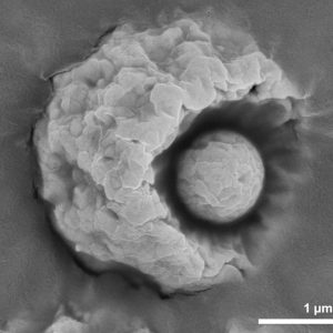
Cutting out a filter contained in a single-use mask to keep us safe during the global coronavirus pandemic. SEM Merlin.
Pyrite (FeS2) particle surface after calcination at 800°C. During the process, pyrite decomposes releasing SO2 gas and transforms into iron oxide. The process sometimes involves some degree of melting, resulting in the liquid-like morphology observed here. Particle mounted in carbon film, coated with 4nm Ir. GeminiSEM 300.
Carboaluminate (AFm) precipitated in the shape of a surfer “riding” a grain of un-hydrated cement and surrounded by C-A-S-H. Polished section of LC3. SEM Merlin.
Kaolinite particle mounted over carbon film, coated with 4nm Ir, showing the multiple layers that form the clay’s particle structure and gives them their characteristic high surface area. GeminiSEM 300.

A failed yet beautiful attempt towards the optimization of poly(triazine imide) membranes. We deposited single-layer poly(triazine imide)nanosheets on a porous alumina support. Microscope: SEM Teneo.

Assembly of gold nanoparticles on a ceramic nanofiber. TEM Talos.
The image is from a polished surface of natural aggregate. GeminiSEM 300.
March/April 2021 competitors
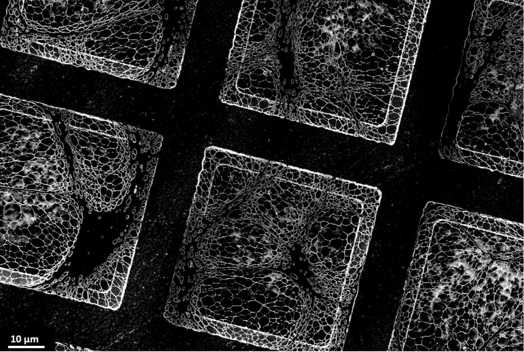
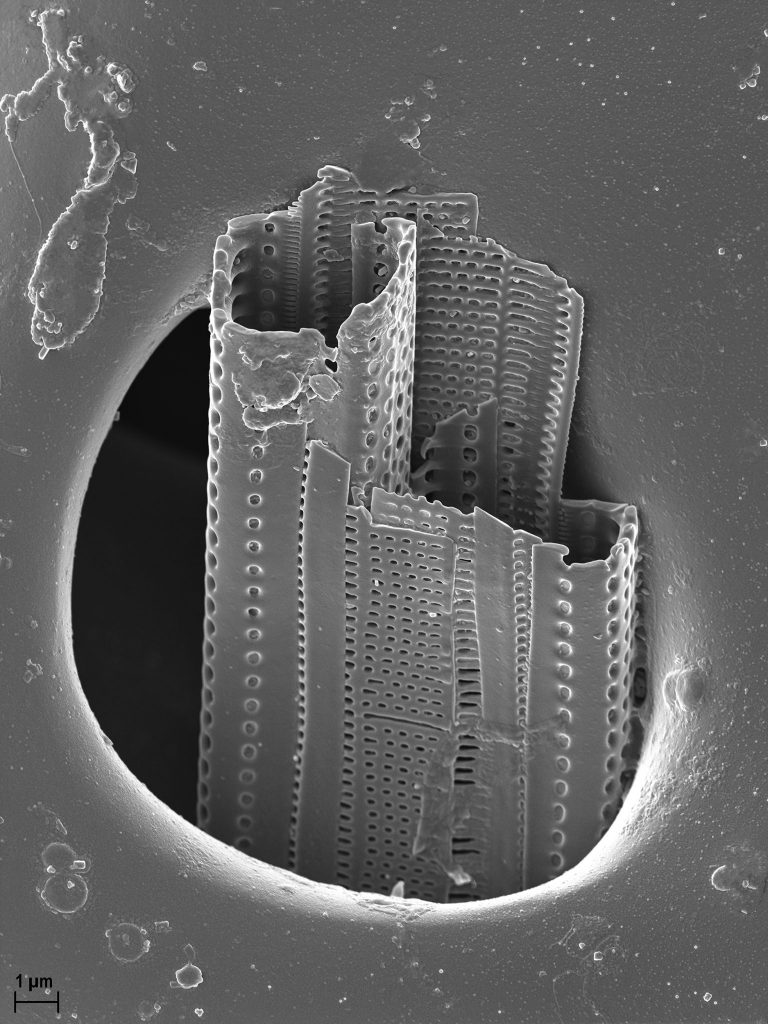
Particles deposited on TEM grid, observed by SEM after TEM imaging. (The image isn’t enough magnified and only show the nice tem grid). Microscope: SEM Gemini. 1/6
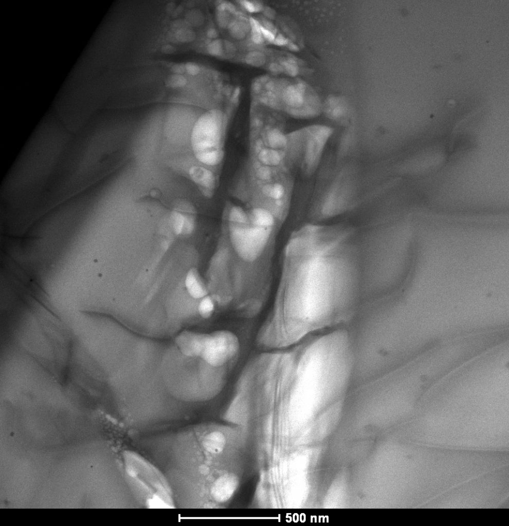
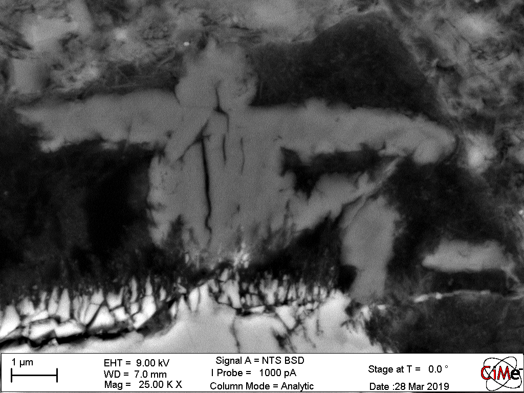
Alkali-Silica Reaction (ASR) caught red-handed cracking an aggregate in a concrete sample at early age (4 weeks). Microscope: TEM Osiris. 2/6
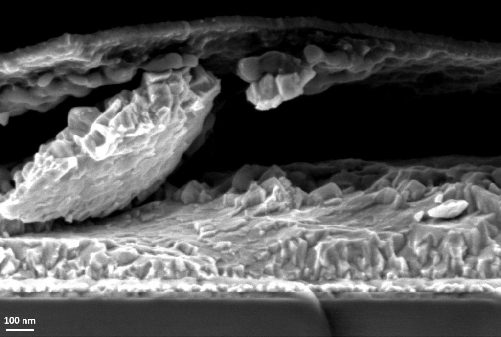
FTO deposited on glass substrate broke and lifted the upper layer deposited on it (cross section imaging). Microscope: SEM Gemini. 3/6
Formation of silico-alkali-calcareous “hedgehogs” in concrete immersed for 3 months in an alkaline solution. Microscope: SEM Merlin. 4/6
Molybdenum disulfide (MoS2) are classified as transition metal dichalcogenides (TMDS) materials. The hexagonal crystal structure of MoS2is formed by the sandwiched Mo atomic planes between the S atomic layers on both sides. Due to the large direct bandgap and high carrier mobility, it makes an obvious choice to use it for device applications or beyond electronics such as Valleytronics. Atomic resolution imaging and spectroscopy remains a challenge for these materials. Due to the complex defect formation mechanism, TMDs are very sensitive to electron beam irradiation and may change the structures permanently. Here, it shows the holes formations in the monolayer MoS2 during the energy dispersive spectroscopy. Microscope: TEM Themis. 5/6
Cross section of various thin films deposited on top of a glass-FTO substrate. A ”tree” grew probably as a scratch effect when breaking the glass in 2 pieces. Microscope: SEM Gemini. 6/6
Particles deposited on TEM grid, observed by SEM after TEM imaging. (The image isn’t enough magnified and only show the nice tem grid). Microscope: SEM Gemini.
Alkali-Silica Reaction (ASR) caught red-handed cracking an aggregate in a concrete sample at early age (4 weeks). Microscope: TEM Osiris.
FTO deposited on glass substrate broke and lifted the upper layer deposited on it (cross section imaging). Microscope: SEM Gemini.
Formation of silico-alkali-calcareous “hedgehogs” in concrete immersed for 3 months in an alkaline solution. Microscope: SEM Merlin.
Molybdenum disulfide (MoS2) are classified as transition metal dichalcogenides (TMDS) materials. The hexagonal crystal structure of MoS2is formed by the sandwiched Mo atomic planes between the S atomic layers on both sides. Due to the large direct bandgap and high carrier mobility, it makes an obvious choice to use it for device applications or beyond electronics such as Valleytronics. Atomic resolution imaging and spectroscopy remains a challenge for these materials. Due to the complex defect formation mechanism, TMDs are very sensitive to electron beam irradiation and may change the structures permanently. Here, it shows the holes formations in the monolayer MoS2 during the energy dispersive spectroscopy. Microscope: TEM Themis.
Cross section of various thin films deposited on top of a glass-FTO substrate. A ”tree” grew probably as a scratch effect when breaking the glass in 2 pieces. Microscope: SEM Gemini.
January/February 2021 competitors
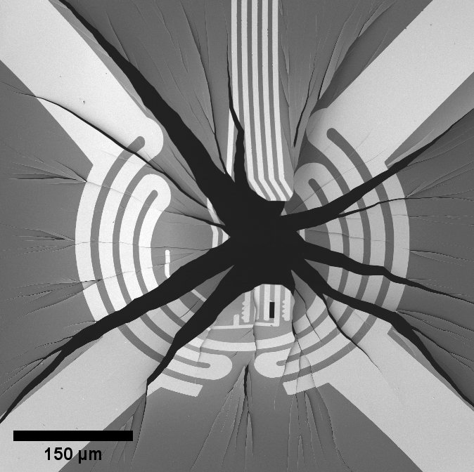
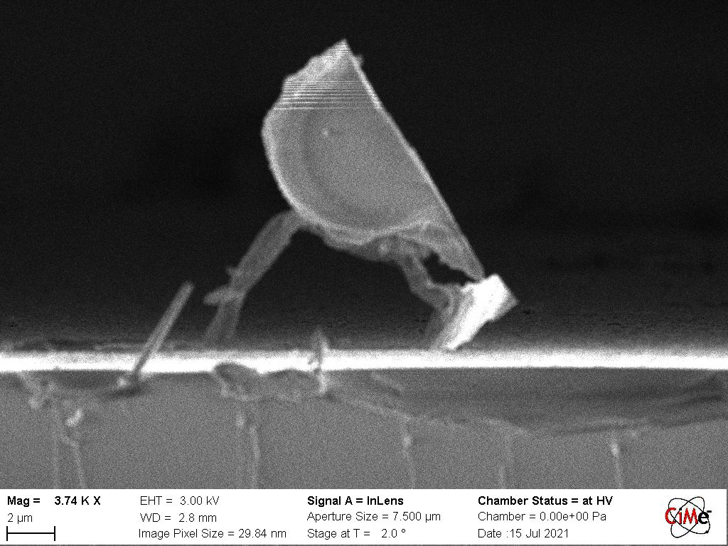
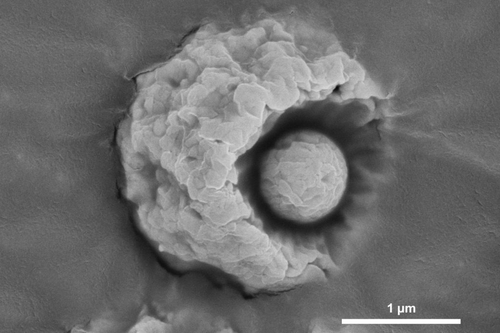
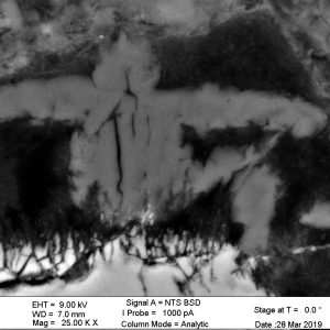
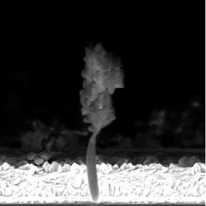
Catastrophic failure of a MEMS device during focused ion beam manipulations. The device is supported on a thin silicon nitride membrane, which, as it turns out, was quite a bit strained. The strain was suddenly released, when the ion beam hit the membrane. Microscope in use: Zeiss NVision 40. 1/15
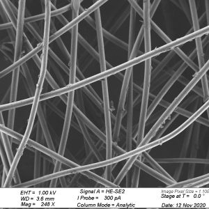
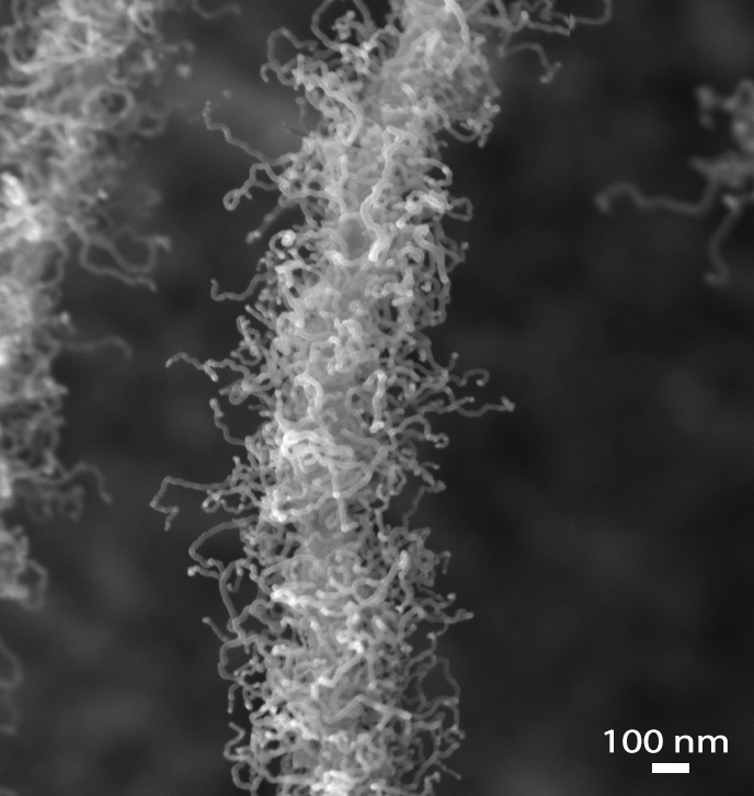
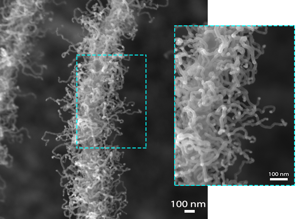
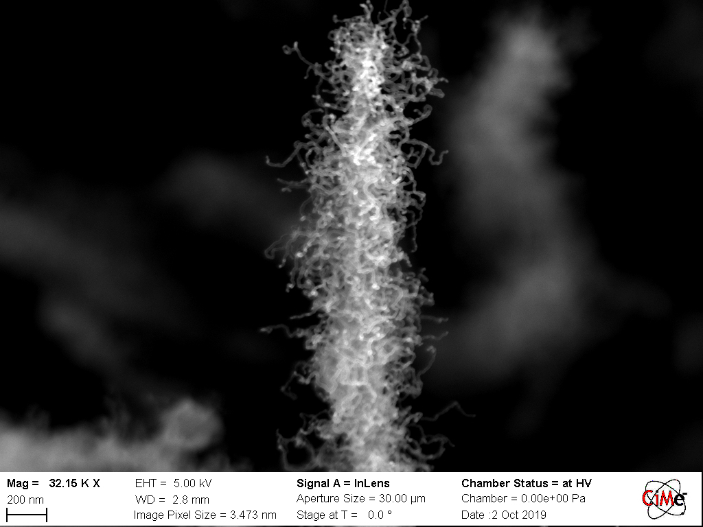
Bacterial biofilm developed on a conductive electrode surface to enhance exoelectrogene bacteria’s population density. In particular geobacter sulfurreducens which is able to convert domestic waste water into electrons. These electrons are then able to travel through biological ‘nanowires’ lattice visible on the picture. We can also observe in the middle of the picture a strange pollen-like structure showing the diversity of populations in waste waters. 2/15
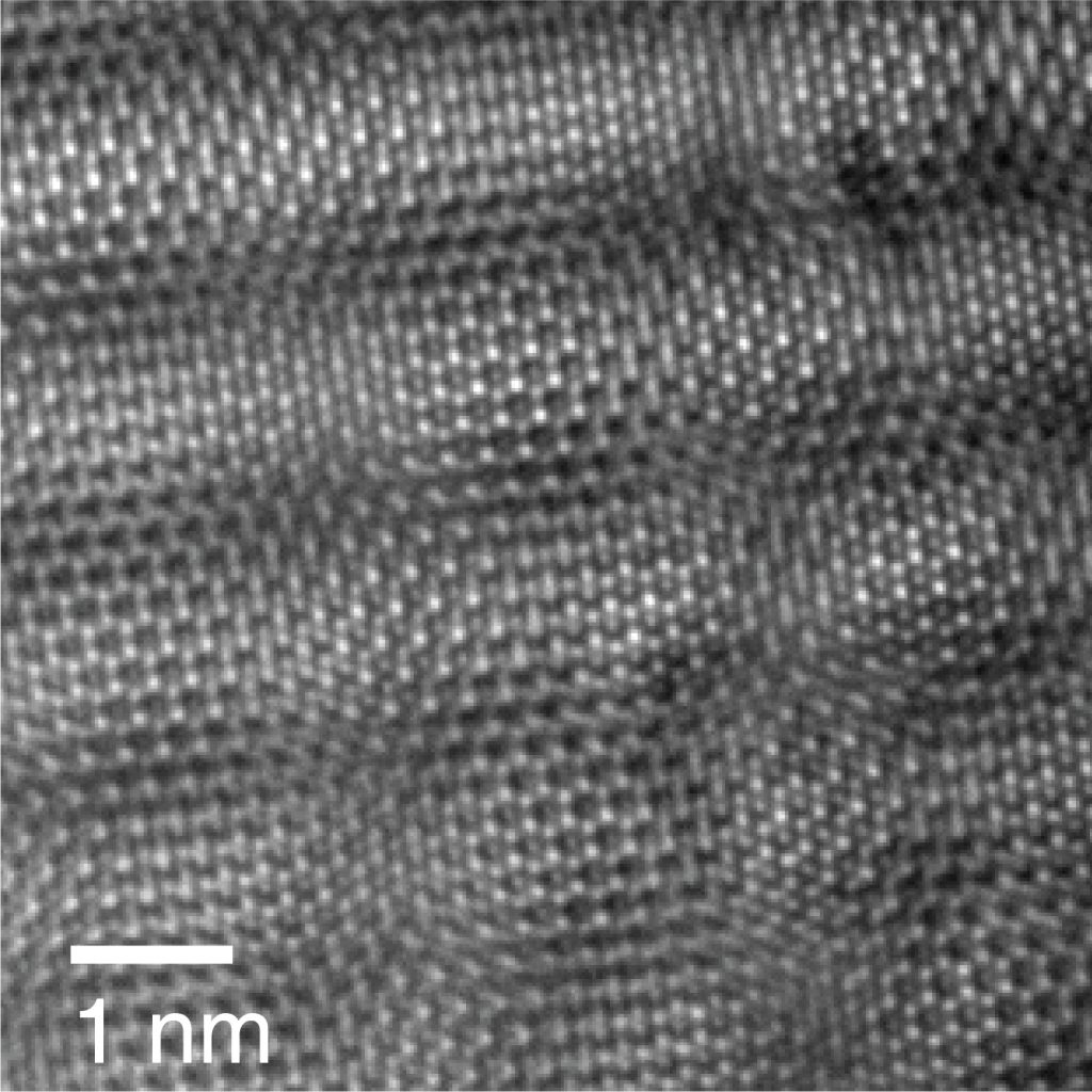
Multilayer graphene grown at low temperatures using Ni as the catalyst and benzene as the carbon precursor. AC-HRTEM taken on the double-corrected Titan Themis 60-300 (FEI) equipped with a Wein-type monochromator. An 80 keV incident electron beam was used to reduce the electron radiation damage. The incident electron beam was monochromated (“rainbow” mode illumination) to reduce the effects of chromatic aberration. 3/15
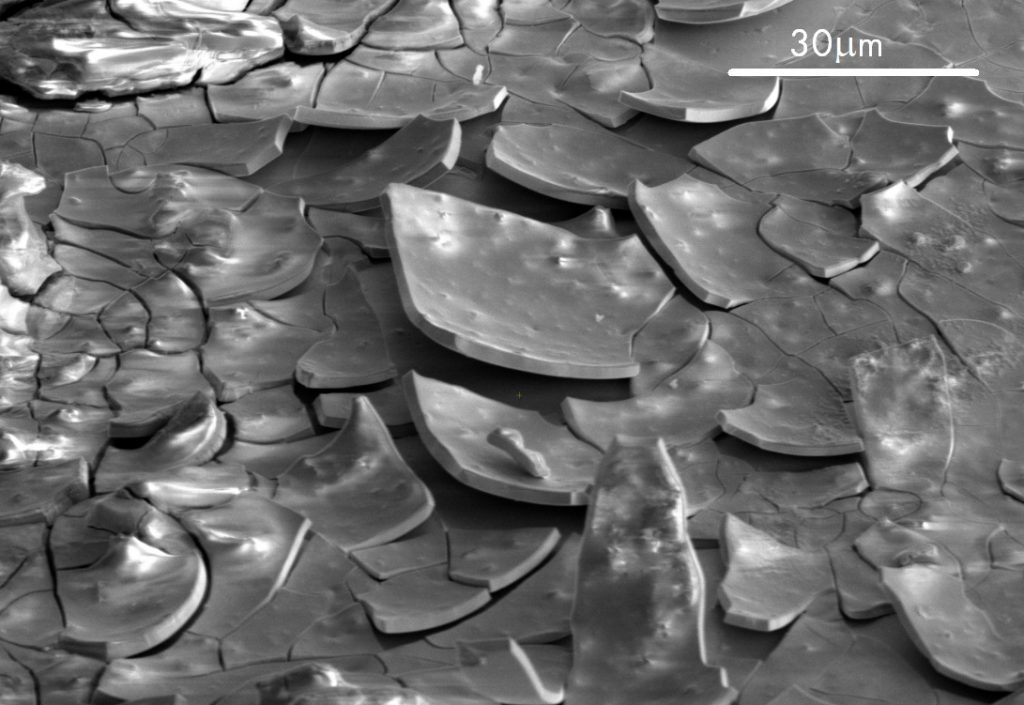
SEM image of the surface of a GdSbTe compound. The surface layer has cracked and bend up similar to soil when it dries out from summer heat. This degradation has only affected the surface layer while the sample underneath remained in tact. The image was taken on the Helios PFIB. 4/15
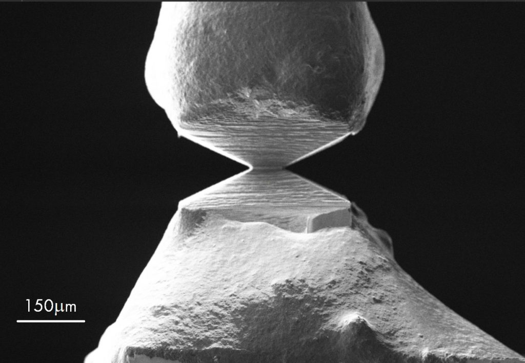
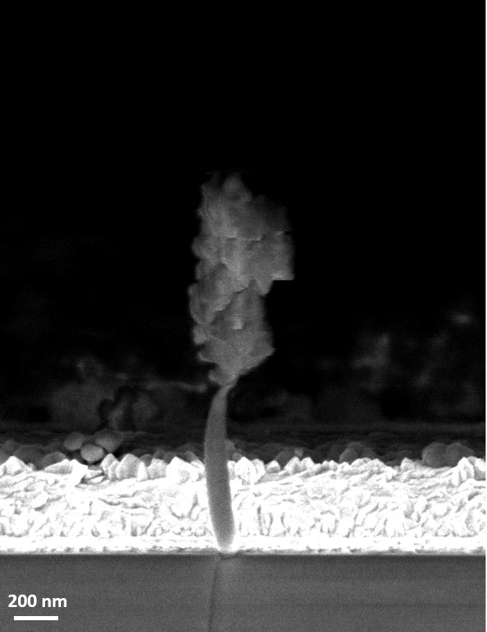
Pillar made on the Helios PFIB. The sample was mounted with silver epoxy and then thinned down to produce a strain lense at which the sample is cleaved later in an STM system at low temperature. 5/15
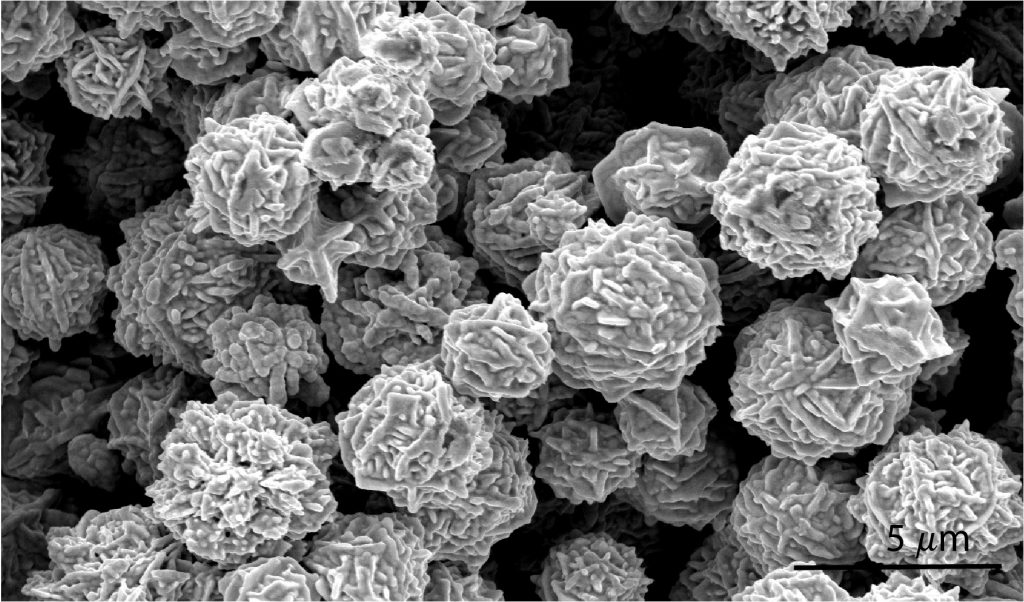
These microparticles are from extremely pure, 100% (24 carats) red gold. They were prepared by an innovative wet chemical method. Their crystallization mechanism is fascinating, leading to the formation of these crystallites which resemble to the scenery of the bottom of the ocean covered with a closely packed sea urchin colony. 6/15
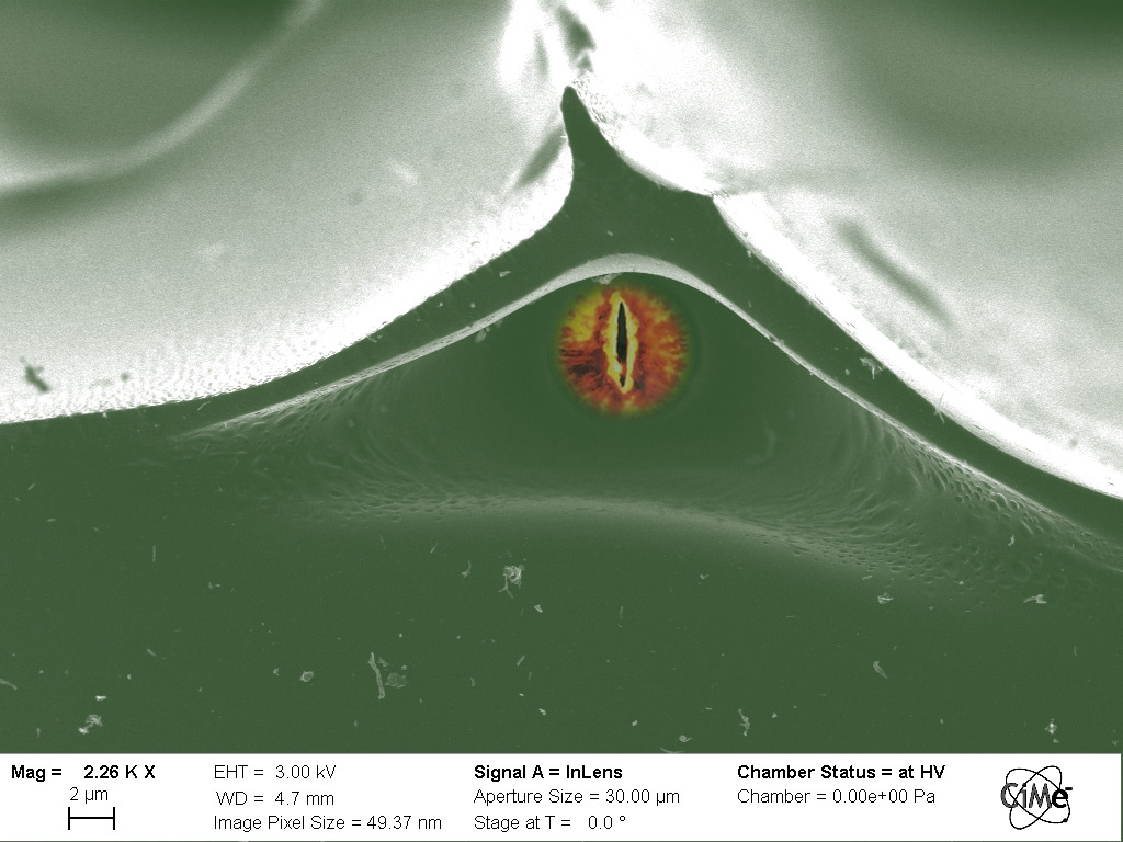
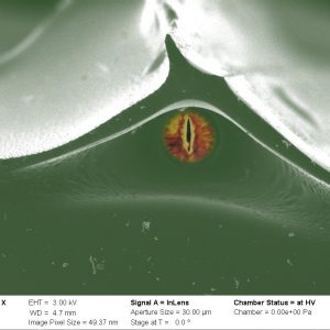
Beauty lies in the eye of the beholder, but sometimes the ugly lies in your sample, staring back at you! An As2Se3 chalcogenide film was thermally evaporated onto a corrugated polymer substrate. The film was then dip-coated for encapsulation. Solvant etched a hole under the corrugated chalcogenide film by error, which was calling for an eye to be photoshopped into it. A cross-section was obtained by cryo-cutting the film in liquid nitrogen at CIME. Observation was made using a wafer section holder in the Gemini SEM. 7/15
Fractured surface of a lead halide perovskite single crystal. This light-sensitive material has been rediscovered recently, and now part of very efficient solar cells and photodetectors prototypes. The image was taken by scanning electron microscope. The micron-sized features on the fractured surface of this high-quality single-crystal magically resembles to what a traveler sees in Switzerland, namely, the scenery of the Swiss Alps during a full moon illuminated winter night. 8/15
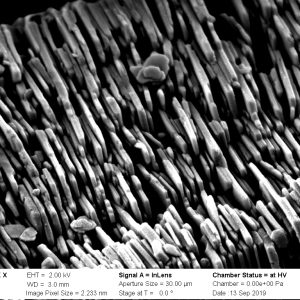
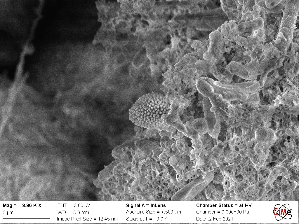
Phytoplancton emerging from a pore on the skeleton of the mediterranean sea urchin Paracentrotus lividus. The function of the many interconnected pores is to allow the passage of adhesive tube feet, mainly for locomotion. This endoskeleton, enclosed by an epidermis, and spines, is called a test. It is famous for its beautiful symmetry, and is mostly made of calcite and magnesite. Its shape is effective at distributing stress evenly over the surface. Marine echinoderms can be studied for their numerous biomimetic applications. Gold coated, and photographed at 2kv on a Gemini-SEM 300. 9/15

Afailed yet beautiful attempt towards the optimization of poly(triazine imide) membranes. We deposited single-layer poly(triazine imide)nanosheets on a porous alumina support. SEM image taken using Sion’s Teneo Microscope . 10/15
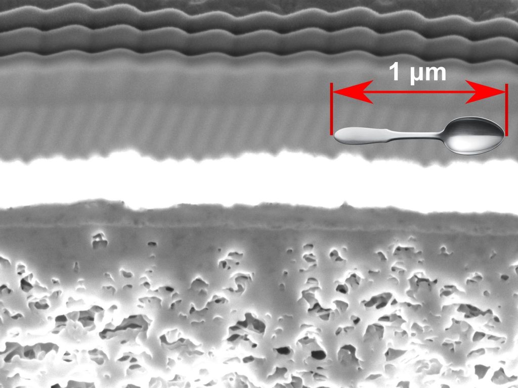
The image was taken with FIB XB450 microscope. It is a cross section where bottom spongy layer is polybenzimidazole polymer followed by a 200 nm-thick zeolite layer on top of which a 300 nm-thck layer of gold was deposited and finally the wavy layers are made out of carbon. 11/15
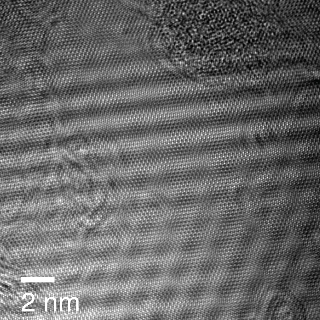
Multilayer graphene grown at low temperatures using Ni as the catalyst and benzene as the carbon precursor. AC-HRTEM taken on the double-corrected Titan Themis 60-300 (FEI) equipped with a Wein-type monochromator. An 80 keV incident electron beam was used to reduce the electron radiation damage. The incident electron beam was monochromated (“rainbow” mode illumination) to reduce the effects of chromatic aberration. 12/15
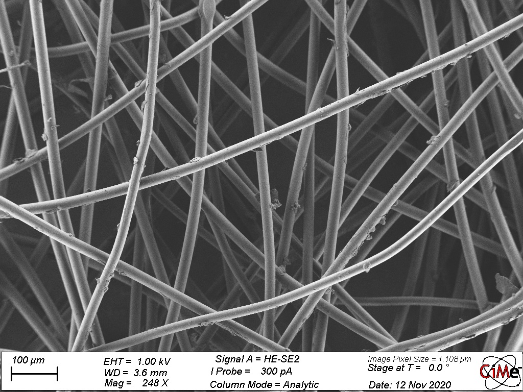
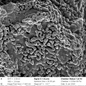
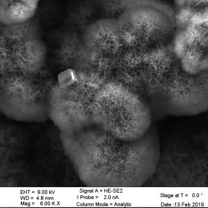
It is known that most cactus species grow in hot, dry regions, but who would have thought that chemical vapor deposition processing at EPFL would provide an optimized condition for the growth of a Cu-CNT nano-cactus forest? In this SEM image, you see an individual Cu nanowire uniformly covered with radially-grown CNTs in a hierarchical cactus-like structure. These individual nano-cactuses were vertically grown in a random forest and can perfectly absorb light in the Vis-to-NIR region. 13/15
It is known that most cactus species grow in hot, dry regions, but who would have thought that chemical vapor deposition processing at EPFL would provide an optimized condition for the growth of a Cu-CNT nano-cactus forest? In this SEM image, you see an individual Cu nanowire uniformly covered with radially-grown CNTs in a hierarchical cactus-like structure. These individual nano-cactuses were vertically grown in a random forest and can perfectly absorb light in the Vis-to-NIR region. 14/15
It is known that most cactus species grow in hot, dry regions, but who would have thought that chemical vapor deposition processing at EPFL would provide an optimized condition for the growth of a Cu-CNT nano-cactus forest? In this SEM image, you see an individual Cu nanowire uniformly covered with radially-grown CNTs in a hierarchical cactus-like structure. These individual nano-cactuses were vertically grown in a random forest and can perfectly absorb light in the Vis-to-NIR region. 15/15
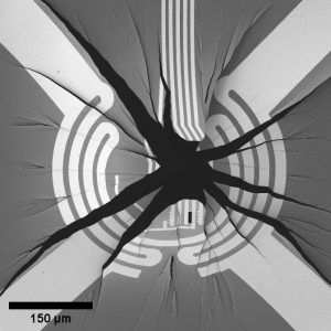
Catastrophic failure of a MEMS device during focused ion beam manipulations. The device is supported on a thin silicon nitride membrane, which, as it turns out, was quite a bit strained. The strain was suddenly released, when the ion beam hit the membrane. Microscope in use: Zeiss NVision 40.
Bacterial biofilm developed on a conductive electrode surface to enhance exoelectrogene bacteria’s population density. In particular geobacter sulfurreducens which is able to convert domestic waste water into electrons. These electrons are then able to travel through biological ‘nanowires’ lattice visible on the picture. We can also observe in the middle of the picture a strange pollen-like structure showing the diversity of populations in waste waters.

Multilayer graphene grown at low temperatures using Ni as the catalyst and benzene as the carbon precursor. AC-HRTEM taken on the double-corrected Titan Themis 60-300 (FEI) equipped with a Wein-type monochromator. An 80 keV incident electron beam was used to reduce the electron radiation damage. The incident electron beam was monochromated (“rainbow” mode illumination) to reduce the effects of chromatic aberration.
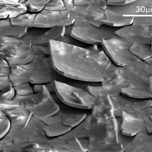
SEM image of the surface of a GdSbTe compound. The surface layer has cracked and bend up similar to soil when it dries out from summer heat. This degradation has only affected the surface layer while the sample underneath remained in tact. The image was taken on the Helios PFIB.
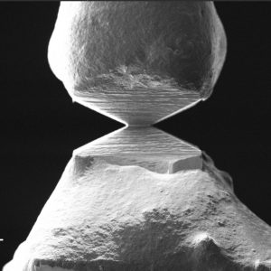
Pillar made on the Helios PFIB. The sample was mounted with silver epoxy and then thinned down to produce a strain lense at which the sample is cleaved later in an STM system at low temperature.
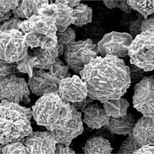
These microparticles are from extremely pure, 100% (24 carats) red gold. They were prepared by an innovative wet chemical method. Their crystallization mechanism is fascinating, leading to the formation of these crystallites which resemble to the scenery of the bottom of the ocean covered with a closely packed sea urchin colony.
Beauty lies in the eye of the beholder, but sometimes the ugly lies in your sample, staring back at you! An As2Se3 chalcogenide film was thermally evaporated onto a corrugated polymer substrate. The film was then dip-coated for encapsulation. Solvant etched a hole under the corrugated chalcogenide film by error, which was calling for an eye to be photoshopped into it. A cross-section was obtained by cryo-cutting the film in liquid nitrogen at CIME. Observation was made using a wafer section holder in the Gemini SEM.
Fractured surface of a lead halide perovskite single crystal. This light-sensitive material has been rediscovered recently, and now part of very efficient solar cells and photodetectors prototypes. The image was taken by scanning electron microscope. The micron-sized features on the fractured surface of this high-quality single-crystal magically resembles to what a traveler sees in Switzerland, namely, the scenery of the Swiss Alps during a full moon illuminated winter night.
Phytoplancton emerging from a pore on the skeleton of the mediterranean sea urchin Paracentrotus lividus. The function of the many interconnected pores is to allow the passage of adhesive tube feet, mainly for locomotion. This endoskeleton, enclosed by an epidermis, and spines, is called a test. It is famous for its beautiful symmetry, and is mostly made of calcite and magnesite. Its shape is effective at distributing stress evenly over the surface. Marine echinoderms can be studied for their numerous biomimetic applications. Gold coated, and photographed at 2kv on a Gemini-SEM 300.

Afailed yet beautiful attempt towards the optimization of poly(triazine imide) membranes. We deposited single-layer poly(triazine imide)nanosheets on a porous alumina support. SEM image taken using Sion’s Teneo Microscope .
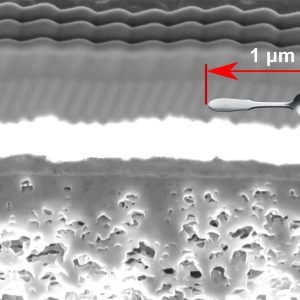
The image was taken with FIB XB450 microscope. It is a cross section where bottom spongy layer is polybenzimidazole polymer followed by a 200 nm-thick zeolite layer on top of which a 300 nm-thck layer of gold was deposited and finally the wavy layers are made out of carbon.
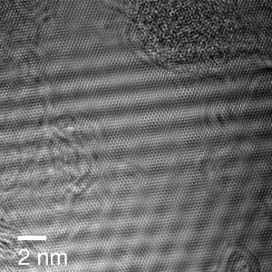
Multilayer graphene grown at low temperatures using Ni as the catalyst and benzene as the carbon precursor. AC-HRTEM taken on the double-corrected Titan Themis 60-300 (FEI) equipped with a Wein-type monochromator. An 80 keV incident electron beam was used to reduce the electron radiation damage. The incident electron beam was monochromated (“rainbow” mode illumination) to reduce the effects of chromatic aberration.
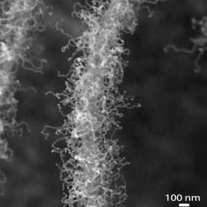
It is known that most cactus species grow in hot, dry regions, but who would have thought that chemical vapor deposition processing at EPFL would provide an optimized condition for the growth of a Cu-CNT nano-cactus forest? In this SEM image, you see an individual Cu nanowire uniformly covered with radially-grown CNTs in a hierarchical cactus-like structure. These individual nano-cactuses were vertically grown in a random forest and can perfectly absorb light in the Vis-to-NIR region.
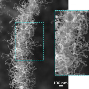
It is known that most cactus species grow in hot, dry regions, but who would have thought that chemical vapor deposition processing at EPFL would provide an optimized condition for the growth of a Cu-CNT nano-cactus forest? In this SEM image, you see an individual Cu nanowire uniformly covered with radially-grown CNTs in a hierarchical cactus-like structure. These individual nano-cactuses were vertically grown in a random forest and can perfectly absorb light in the Vis-to-NIR region.
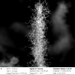
It is known that most cactus species grow in hot, dry regions, but who would have thought that chemical vapor deposition processing at EPFL would provide an optimized condition for the growth of a Cu-CNT nano-cactus forest? In this SEM image, you see an individual Cu nanowire uniformly covered with radially-grown CNTs in a hierarchical cactus-like structure. These individual nano-cactuses were vertically grown in a random forest and can perfectly absorb light in the Vis-to-NIR region.