Back to the current year Winners
2021, December
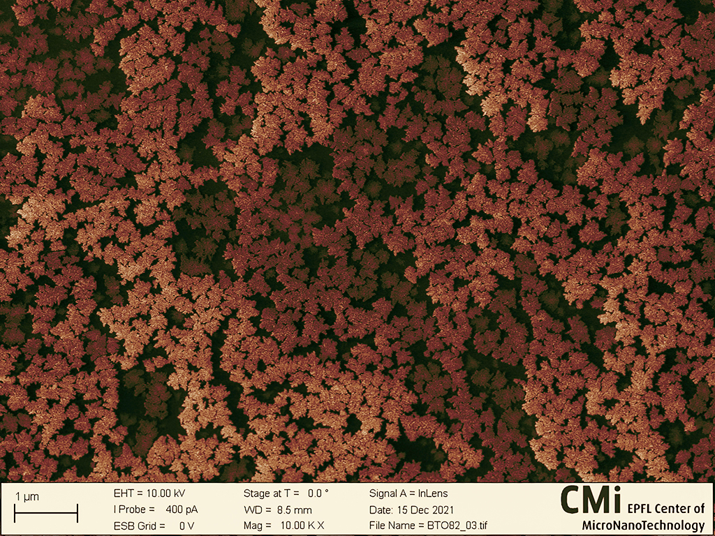
Autumn
Wojciech Szmyt, LPMAT
The SEM image shows BaTiO3 crystallites, with a warm gradient colormap for this autumn feel.
2021, November

Micro Eclipse
Amir Youssefi, LPQM
A superconducting quantum memory in the dark field!
2021, October

Couleurs d’automne
Clémentine Lipp, LMIS4
The process for the fabrication of glass buried micro-channels has more than one trick in the pocket. While the reason behind the colors emerging from these glass structures is still a mystery, their beautiful color palette remains mesmerizing.
2021, September

The Empire strikes back!
Seniz Küçük, NEMS
Yet another star destroyer has been spotted in the CMI cleanroom. The Empire seems to be using crystalline orientation to hide the ship’s shield generators this time. The mysterious structure, which is suspected to be Mo, has appeared after Mo etching in IBE which is then followed by HF cleaning.
2021, August
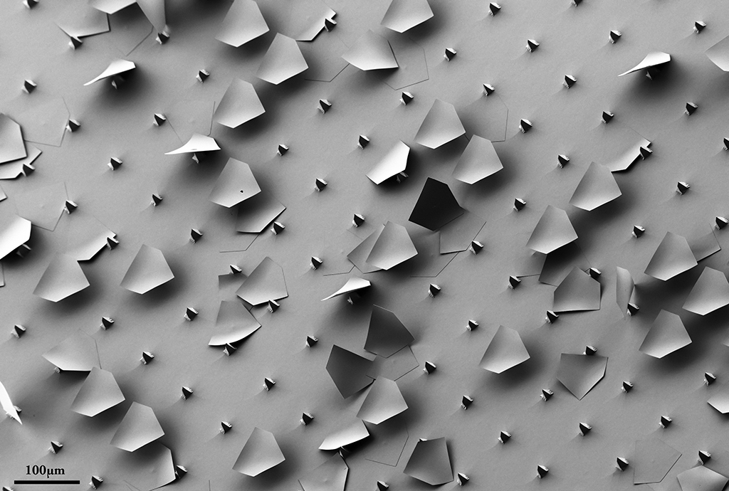
Paper Planes in a Mine Field
Matthias Neuenschwander, LBNI
A swarm of paper planes has mistakenly landed in a mine field, with dramatic consequences. When a pentagonal silicon oxide mask is under-etched using KOH, very sharp silicon tips can be formed. If the under-etch is incomplete however, the mask can remain partially attached to the silicon tip.
2021, July
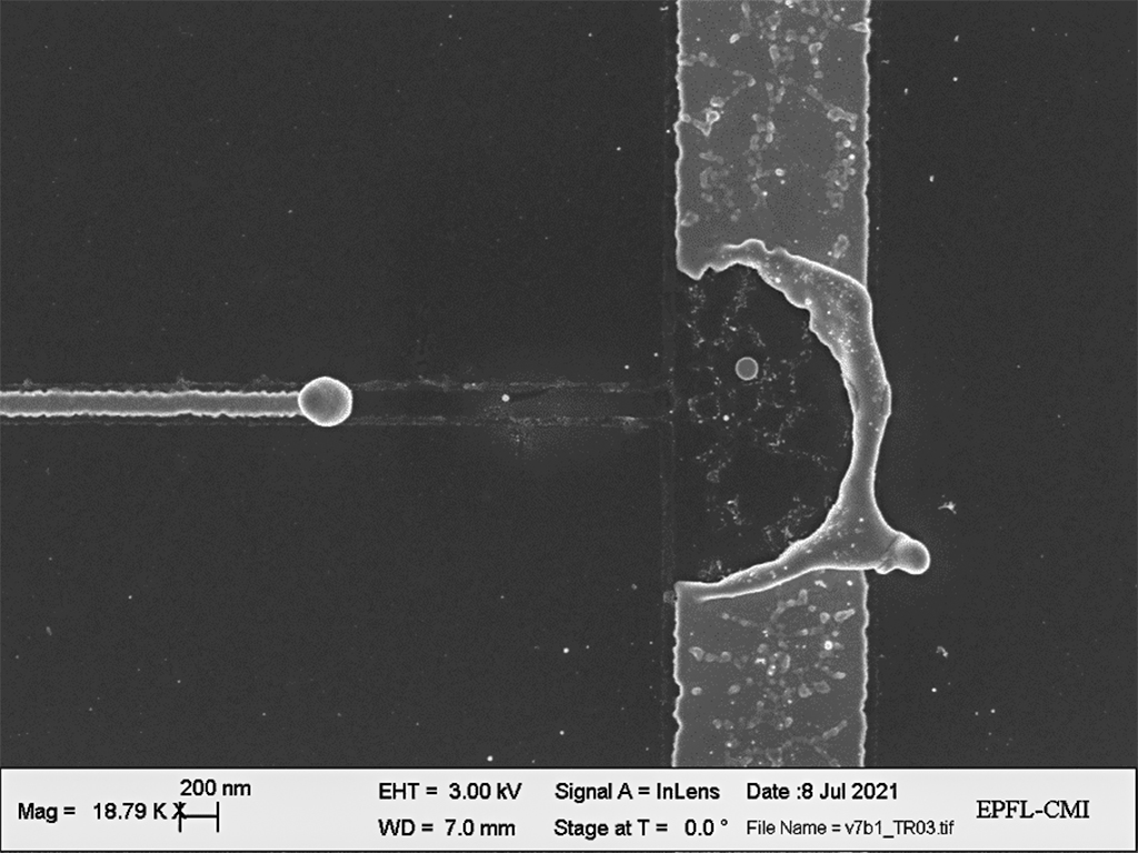
Nanoscale explosion
Marco Riccardi, NAM
Built-in stress in this high-surface-area and high-aspect-ratio gold structure leads to “explosions” around its weakest points (right angle junctions), where the gold tries to reorganize into more favorable spherical shapes.
2021, June
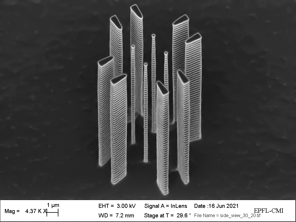
Don’t lean out of these skyscrapers, you may suffer from vertigo!
Vincenzo Messina, ANEMS
These ultra-modern skyscrapers are built by etching silicon. The results are structures with an aspect ratio that even the most amazing skyscrapers in New York envy.
2021, May
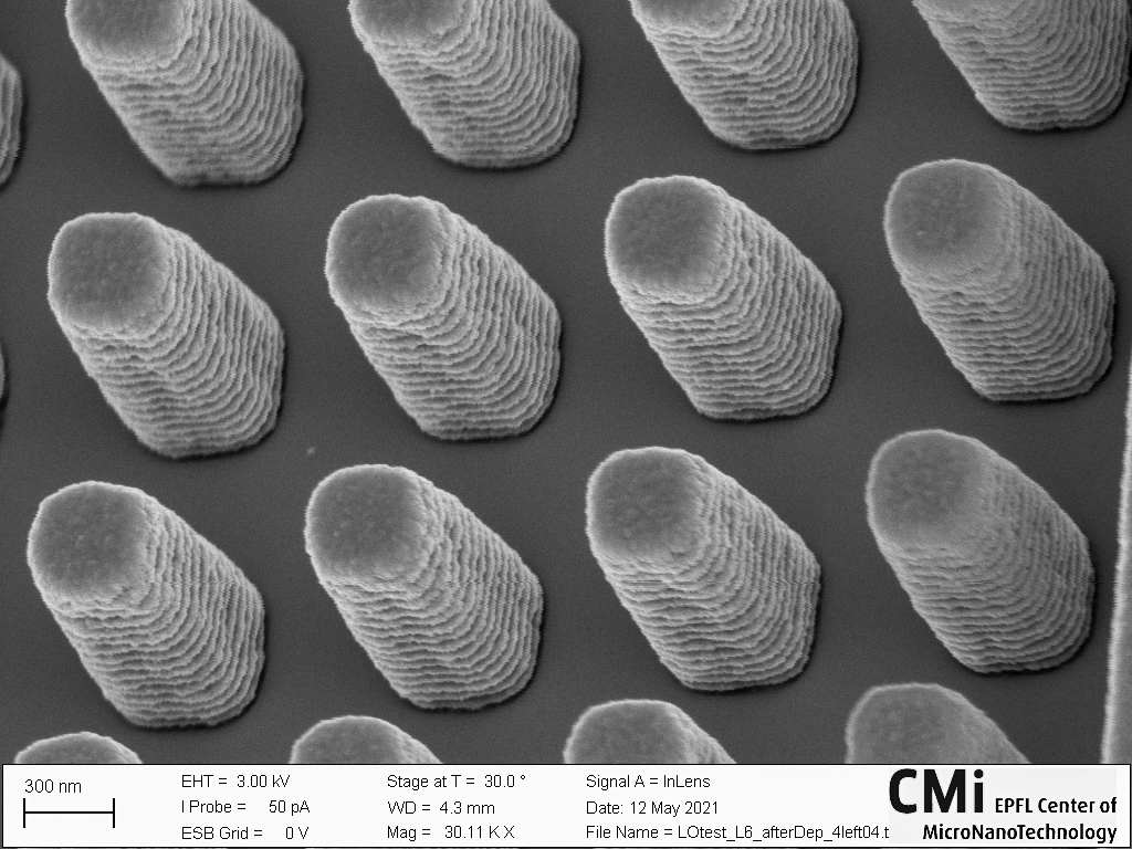
Those Nano-stalagmites are growing fast!
Francesco Bertot, Q-lab
Stalagmites are created by water droplets that deposit minerals on the ground, but these nano-samples are obtained sputtering a thin film of GeTe over a developed photoresist. The combination of the resist sidewalls and the deposited material creates this peculiar effect, in which it seems that multiple layers have been deposited and patterned one on top of the other.
2021, April
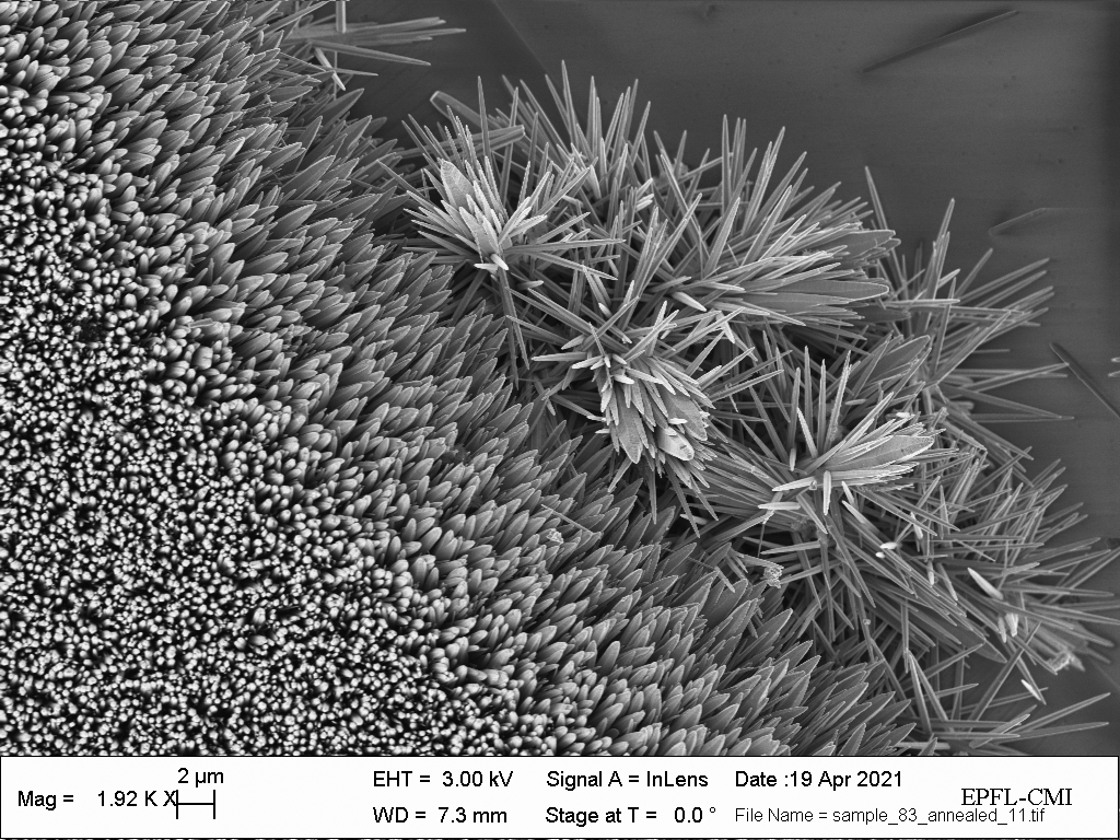
The power of ZnO nanowires transformation
Enrico Bertero, H.Glass
As a strong wave changes shape during its path and at the end sprays when in contact with the shore, in this case ZnO nanowires transform from highly ordered and vertical wires, to tilted rods and finally to flower-like wires blossoming at the edge of the substrate.
2021, March
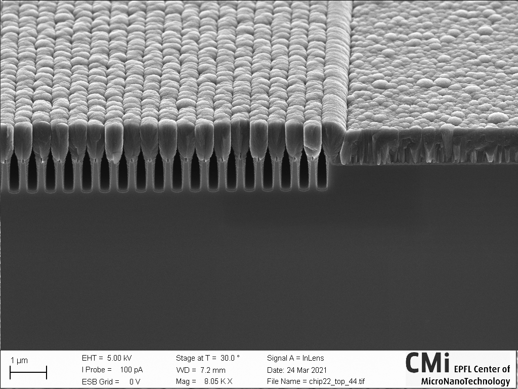
Silicon forest
Sylvain Mario El-Khoury, Q-LAB
Those trees are finally ready to be cut by the CMi lumberjacks ! For the curious, their trunk is made of c-Si, their bark is SiO2 (PECVD) and the leaves are a-Si (sputtered).
2021, February
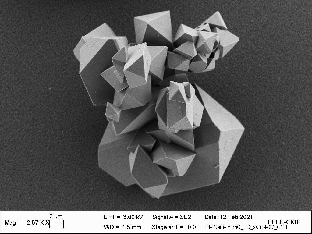
Multi-faceted ZnO crystal on a see of nanowires
Enrico Bertero, H.Glass
Getting lost in the facets and edges of such beautiful ZnO grains is easy. But, by focusing only on that, we miss in definition of what is below it. Indeed, it is a vast sea of compact ZnO nanowires, supporting this ZnO structure, like a distorted pyramid floating above a desert of needles.
2021, January
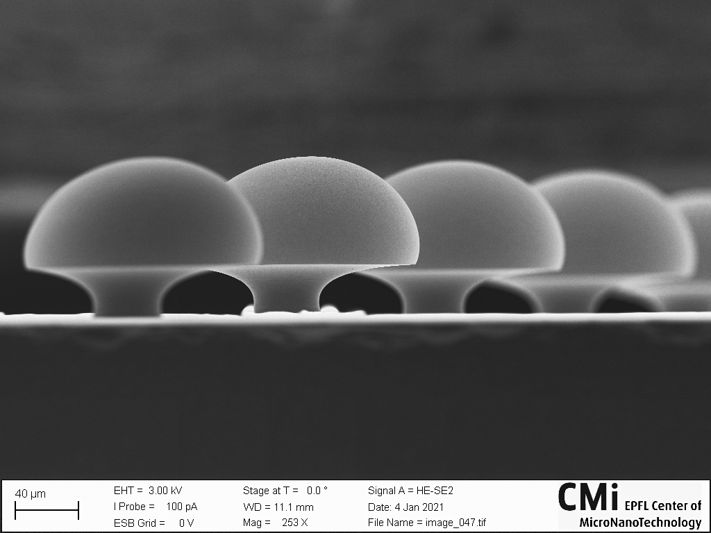
Fungal Infestation in CMi?!
Alain Takabayashi, Q-LAB
It is known that mushrooms grow in damp, dark places, but who would have thought that the wet processing in Z19 would produce the conditions that allowed these copper champignons to grow? Fear not, though, the cleanliness of the zone has not been compromised! These structures are in fact electroplated copper structures (originally intended to be pillars) on a sputtered gold seed layer that have overgrown the confines of a 40 μm thick photoresist.