AZ P4K-AP is used in CMi as a protective coating for dicing. The resist is not photosensitive and therefore cannot be exposed to be patterned. For protection, please coat a layer thicker than your bigger structure. If AZ P4K-AP cannot be thick enough to protect your structure, use the AZ 10XT-60 instead.
Wafer surface preparation
Usually adhesion of photoresist on inorganic materials is poor resulting in losses of fine structures after development. To solve the issue, silicon wafers are generally treated using the HMDS vapor prime treatment before spincoating the photoresist. Details about the HMDS process and control can be found here: link
Assuming wafers with a clean surface free of organic contamination, the best adhesion will be obtained with the surface preparation recommended in the table:
| Surface material (larger area) | Vapor HMDS | Plasma O2 | Thermal dehydratation |
|---|---|---|---|
| Si | √√ | √ | √ |
| SiO2, fused silica, SiN, Si3N4 | √√ | √ | √ |
| Float glass, pyrex | √ | √√ | √ |
| Metals: Al, Au, Pt, Ti | … | √ | √√ |
| Metals: Ag, Cu, Cr, Fe | … | X | √√ |
| III/V semiconductors (GaN, GaAs) | … | X | √√ |
Legend: √√ Strongly recommended / √ Alternative process / … Not effective / X May affect or destroy underlaying material
Spincoating
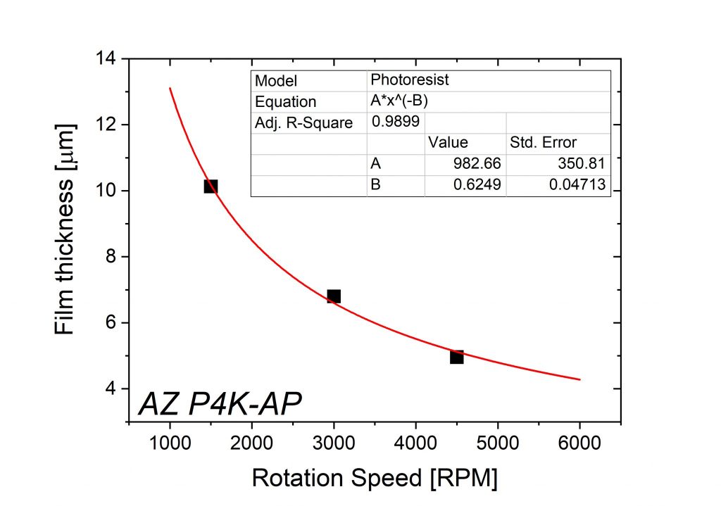
The AZ P4K-AP spincurve is shown below, as well as process details for manual coating.
Manual coating on Sawatec SM-200 :
- Find the spin-coating speed “XXXX” [RPM] matching your target thickness from the AZ P4K-AP spincurve.
- When coating on wafers, use the STD_”XXXX” recipe, which includes a 500 RPM spreading step and 40 seconds of main coating step.
- When coating on small chips, use the CHIP_”XXXX” recipe, which includes 40 seconds of main coating step and a short acceleration at the end to reduce edge bead effects.
- Softbake temperature: 125°C
- Softbake time: 1min/um