Table of content
Introduction
Photolithography is a sequence of processing steps which allows to deposit and pattern a photosensitve polymer thin film, the photoresist, on a substrate.
The photoresist (PR) is selectively exposed to ultraviolet (UV) light, triggering a photoreaction that modify its solubility in aqueous base (developer) solutions.
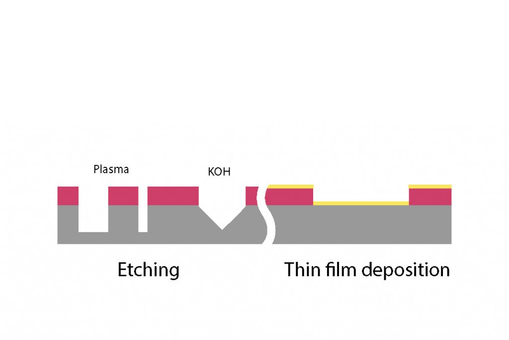
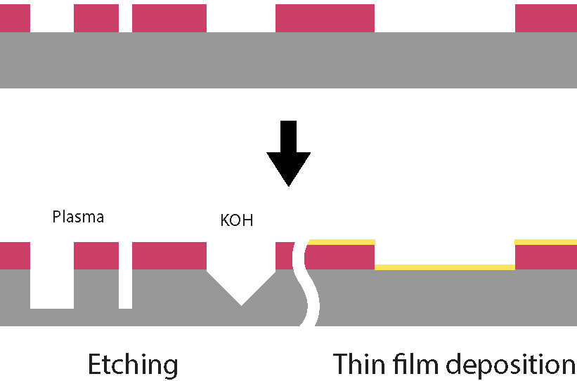
The resulting photoresist pattern is generally used as a mask for the consecutive additive (lift-off) or substractive (etching) processing steps, before being removed (stripped).
I – Photoresist chemistry
Before going into details, we should make a clear distinction between two families of photoresists: Depending on the chemical formulation of the photoresist and the nature of the photoreactions, the solubility of the photoresists in the developer can be either increased (positive-tone PR) or decreased (negative tone PR).
In positive photoresists, the exposed areas become more soluble when subjected to UV light or other radiation. This allows the exposed regions to be washed away during development, leaving behind the unexposed areas as the pattern.
In contrast, negative photoresists undergo cross-linking when exposed to light, making the exposed regions more resistant to dissolution. As a result, the unexposed areas are washed away during development, leaving the hardened exposed pattern intact.
Some of the main differences between the two are the sidewalls slope, resistance to etching, resolution, adhesion to the substrate, etc..

Historically, the first commercial photoresist used for integrated circuits (IC) fabrication was made by Kodak and was branded KTFR, for “Kodak Thin Film Resist”. It was a negative photoresist, that could be tailored to absorb UV light from ~300nm to ~435nm.
From 1972, due to its limited resolution power (minimum critical dimension (CD) ~ 2μm), KTFR was phased out and replaced by the second generation of (positive) photoresists, based on novolak/DNQ material.
Over the years, the advancement of the IC manufacturing processes followed the Moore’s law, which observes that the number of transistors on microchips is doubling every two years. In order to follow this miniaturization trend: Manufacturing processes are scaled down to smaller and smaller design “nodes” (the lateral dimension of the active transistor channel); New photolithography equipment are developed, with a particular focus on reducing the exposure wavelength; New generation of photoresists, with completely different chemical composition, are introduced to the market, with absorption properties matched to the exposure wavelength.
For photoresists, the generations can be summarized in this way:
- i-line photoresists: absorption from ~350nm to ~450nm
- DUV (KrF) photoresists: absorption @ 248nm
- ArF photoresists: absorption @ 193nm
- Extreme UV (EUV) photoresists: absorption @ 13 nm
Regarding chemical composition, photoresists are composed of the following components:
The polymer provides the physical characteristics of the film (density, refractive index, thermal and physical resistance). The most common polymer for i-line lithography is novolak, a molecule based on phenol and formaldehyde groups. For DUV lithography, the polymer molecules are poly-hydroxystyrenes (PHS). For ArF lithography, the polymer materials are much more diversed but the backbone is usually a combination of methyl methacrylate (MMA), t-butylmethacrylate (TBMA), and methacrylic acid (MAA).
Also referred as photoactive compound (PAC) or photoacid generator (PAG), this component absorbs photons and initiate the photoreaction. It transforms into an acid, or helps to generate an acid compound that can directly, or after reaction with other components, modify the solubility of the base polymer in the developper. The other components that can be part of the photoreaction are:
- Quencher: The quencher directly interact with the photoactive compound to limit its reactivity and, in particular, to avoid diffusion of the photoreaction into unexposed area of the photoresist (dark erosion). The quencher allows to fine-tune the photoresist sensitivity and contrast and is a crucial component to achieve high resolution in positive i-line photoresists.
- Cross-linker: The cross-linking agent is the main component of negative photoresists. In the presence of the acid environment generated by the photoreaction, it reacts and binds with the base polymer to form a stronger network. Consequently the exposed area becomes insoluble in the developer. The cross-linking reaction is usually thermally driven and a PEB is required.
-
Chemical amplifier: Chemical “amplification” is a key concept of advanced photoresist, in which the initial absorbed photon generates a strong acid that can catalyze many photoreactions, not just a single one. It was initially developed for DUV photoresists, to improve the imaging performance (higher sensitivity, higher resolution, lower line-edge roughness (LER)). Chemical amplification is usually thermally driven and a PEB is required.
The solvent dilutes the polymer to liquid form to use with spin-coating deposition methods. Propylene glycol methyl ether acetate (PGMEA) is generally used for UV resists, and ethyl lactate is added for DUV resists.
Additional molecules can be present in the formulation: surfactants to improve the coating uniformity and PR adhesion to the substrate, stabilizers to extend the shelf life, plasticiters to modify the mechanical properties of the film…
More information on the chemistry of photoresists are available at this page.
II – Photolithography steps
From the application to the removal of the photoresist, the photolithography sequence generally includes the following steps :
Surface cleaning:
While the cleanroom environment (filtered air, high gases and chemicals purity) strongly reduces the ammount of substrate surface contamination, the operator should still take steps to ensure that the wafer surface is as clean as possible, prior to applying the photoresist.
Contaminants may be present on the surface as adsorbed metal ions, organic or inorganic elements and gases, discrete or cluster of particles, as well as naturally grown thin films (native oxides). All of these might negatively impact the final device performance.
Several methods are available to clean the wafers but not all of them are effective in removing the different type of contaminants. The most common are RCA (for silicon and fused silica wafers) and piranha (for glass wafers) cleaning.
- RCA: RCA is a series of standard wet cleaning steps:
-
In step 1 (SC-1), wafers are soaked in a solution of hydrogen peroxide, ammonium hydroxide and DI water (NH4OH/H2O2/H2O 1:1:5) heated to 80°C. This step removes particles and organic contaminants (but oxidizes the surface).
-
In step 2 (optional step for silicon wafers only), wafers are soaked in a 10% hydrofluoric acid solution (HF/H2O 1:10). This step removes the native oxide.
- In step 3 (SC-2), wafers are soaked in a solution of hydrogen peroxide, hydrochloric acid and DI water (HCl/H2O2/H2O 1:1:6) heated to 85°C. This step removes ions and metal contaminants.
-
- Piranha: Piranha is a mixture of sulfuric acid, hydrogen peroxide and DI water. It is an alternative to RCA and is very effective in removing organic residues, particles and metal ions from the substrate surface. It is usually the recommended cleaning process for glass wafers (float, borofloat 33, borosilicate,…).
While RCA and piranha are the optimal cleaning methods before entering new batches of bare silicon and glass wafers into the fabrication chain, they may not be compatible with processed wafers, especially those that are patterned with metal stacks. Several alternatives are possible:
- SCROD cleaning: SCROD wet cleaning uses a combination of a highly reactive DI water/ozone (DIO3) solution and diluted HF (DHF) to efficiently clean the surface from organics, particles, adsorbed metals and native oxide. SCROD was initialy developped by Sony as a safe, eco-friendly alternative to RCA and Piranha. SCROD is generally used in single-wafer spin cleaning tools where DIO3 and DHF are alternatively sprayed on the wafer.
- Acetone / IPA / DI water solvent cleaning: Organic contamination, such as grease, photoresist residues, carbon compounds can be cleaned efficiently by soaking wafers into acetone, followed by isopropanol rinse baths. This can be combined with ultrasonic or megasonic agitation to also remove most particles from the surface. As a final step, the wafers can be soaked in DI water that can help to remove ionic species. Although not as effective, this cleaning method does not use any acid solutions.
Surface preparation:
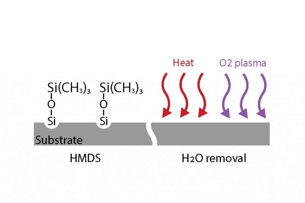
Most inorganic materials used as substrates for microfabrication (silicon, glass) have an hydrophilic surface, and, following the cleaning steps, a certain degree of moisture might be present on the wafer. If the moisture is not removed, the adhesion of the photoresist (PR) to the surface will be insufficient, resulting in the loss of fine structures after development. To solve the issue, wafers should be treated just before applying the PR.
The following standard treatments are available to remove the wafer moisture:
- Dehydration: Dehydration is a simple thermal treatment: The wafers are heated at temperature ranging from 130°C to 160°C for a few minutes and moisture evaporates. This will be the standard preparation method for coating PR on most metallic surfaces.
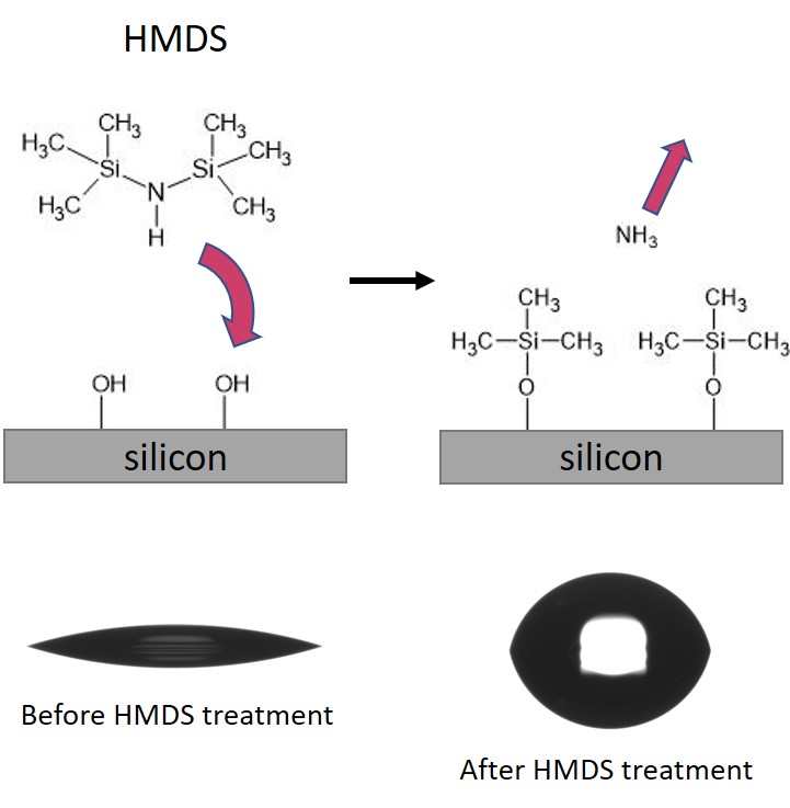
- HMDS: The application of hexamethyldisilazane, [(CH3)3Si]2NH, is an industry standard silanization process, which is used mainly to prepare silicon, SiO2 and Si3N4 surfaces, but can potentially be effective with most oxidized or nitrided surfaces. HMDS is applied from the gas phase on heated substrates (typically 120°C to 150°C). The reaction is depicted below: the silicon atom of the priming agent binds to the oxidized silicon surface leaving hydrophobic methyl groups pointing towards the outside media (air). Consequently the wettability of the surface is affected, and turns from hydrophilic to hydrophobic, as shown in the contact angle snapshots below.
- Plasma O2: Using an oxygen (O2) plasma to treat the wafer surface is an alternative dry-method that can potentially combine the cleaning and surface preparation steps in a single process. Oxygen ions are extremely effective in removing both organic contamination and the humidity. Plasma O2 can not only clean but remove (strip) several microns of spin-coated PR thin films and because of this it is very often used in between the different process steps.
Unfortunately, plasma O2 does not remove particles and metal contaminants from the surface. In addition, the plasma O2 activated surfaces will be extremely hydrophilic and the photoresist coating should be performed without further delays in order to avoid rehydration from the ambiant humidity.
The treatments can also be combined. Due to its efficiency in cleaning organic contaminants, plasma O2 can be performed in most cases, unless the wafer surface is not compatible with oxygen. Then it can be followed by the most efficienct treatment between dehydration and HMDS , depending on the nature of the surface.
To clear the substrate of surface contaminants and humidity.
Spincoating is one of the many techniques used to deposit a photoresist (PR) and, in extension, any diluted polymer uniformly on a substrate. It is usually the ideal solution when working with flat SEMI wafers. Alternative coating methods include dip coating which is mainly used to coat large square substrates (flat panels), and spray coating which is advantageous when the wafer surface has a strong topography.
First, it should be noted that most of the modern spincoating equipment will include specific modules to perform either a dehydration or HMDS surface preparation step.
Coating
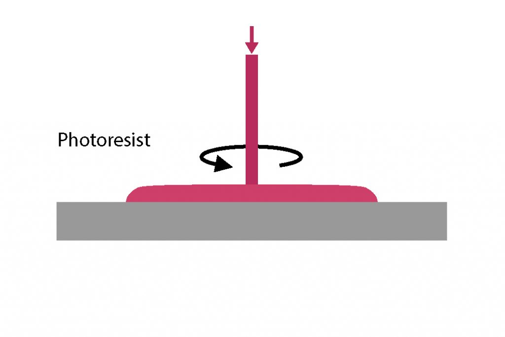
Following the surface preparation, the sequence continues in the spin coating module: a small amount of PR, typically a few mililiter, is dispensed to the center of the substrate, which can be standing still (static dispense) or already spinning (dynamic dispense). The substrate is then rotated, first at an intermediate speed ranging from 500 RPM to 1000 RPM to spread the photoresist by centrifugal force, and then at speeds ranging from 1000 RPM up to 6000 RPM to thin it down to the target thickness.
Soft bake
After coating, the resulting resist thin film will still contain between 20–40% by weight of solvent. To further stabilize the resist film, the coated wafer will be baked for a few minutes at temperature ranging from 90°C to 120°C, effectively removing the excess solvent through evaporation, down to about 3-8% by weight. After the softbake, the photoresist reaches its final thickness, its adhesion to the substrate is improved, and it is now dry enough to be handled without risks of equipment contamination.
The softbake conditions will strongly affect the exposure parameters of the resist. Since it can also negatively impact the PR by potentially promoting the decomposition of the photosensitive compound, and crosslinking/oxidating compounds in the resist. A tradeoff must be found regarding the temperature and duration of the bake to reach optimal and stable process conditions.
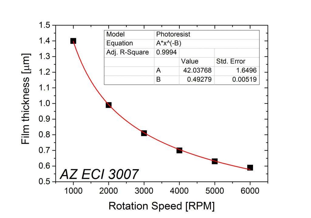
In the end of the whole sequence, the two factors that will have the most impact on the final thickness of the photoresist are the photoresist initial viscosity and the rotation speed in the spincoating unit.
Consequently, the photoresist end user will only be able to change the spincoating speed, and this is why the photoresists are usually described by a spin-curve as shown below.
When using automatic spincoating equipment, some additional options can be included in the spincoating sequence :
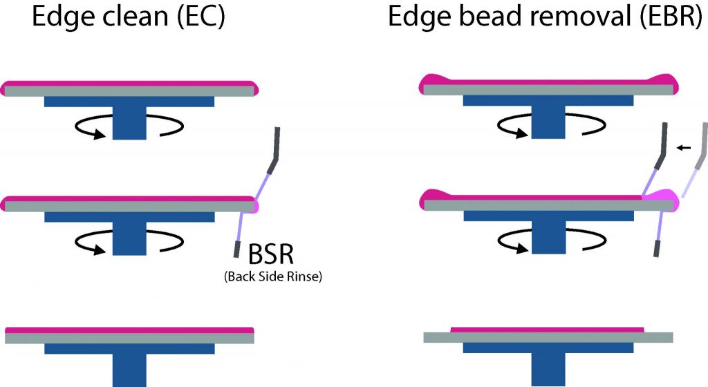
- Backside rinse: As the substrate spins, the PR may migrate or splash onto the back of the substrate. To properly maintain the wafer backside as clean as possible, a solvent rinse is applied from a backside nozzle, while the wafer is still spinning.
- Edge Clean (EC): Combined with the backside rinse, the EC aim at cleaning the edge of the wafer where PR might be present. It is performed by a solvent nozzle mounted on the dispense arm.
- Edge Bead Removal (EBR): Combined with the backside rinse, the EBR is often performed on thick layers of PR (>5um) to remove excess material that has accumulated at the last 3-5mm from the edge of the wafer. The EBR is recommended mainly when using a mask-aligner as exposure equipment (see next section) to maintain a constant gap between the mask and the wafer over the whole surface.
To apply the photoresist on the substrate.
Once the photoresist has been applied to the substrate and baked, it needs to be exposed selectively to light. The exposure triggers a chain of chemical reactions in the photoresist, to make it either soluble or insoluble in an aqueous developer solution.
The following types of equipment are used to expose the photoresist:
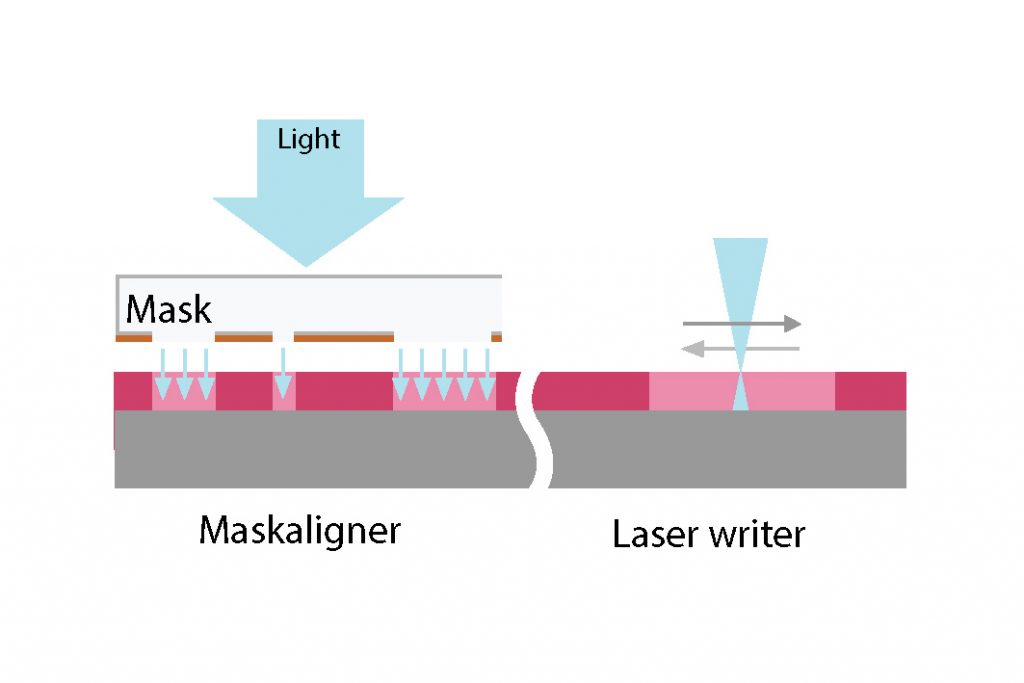
Mask-aligner :
Mask-aligners are the oldest type of exposure equipment. The first commercial mask-aligner was introduced in 1965 by Kulick & Soffa, and then the market was dominated by companies such as Kasper, Cobilt and Canon for the next ~20 years. Mask-aligners are robust, fast, reliable, and cost-effective and, for this reason, they are still in use to this date, mainly for R&D and small-scale production devices.
The mask is a UV-transparent glass or quartz square plate coated with an opaque material, usually chromium. During the mask fabrication process, the wafer layout pattern is precisely transferred into the chromium (more on how to create a mask here). In the mask-aligner, the mask is usually clamped, the wafer is brought in contact or close proximity, precisely aligned thanks to an incorporate microscope, and finally a broad beam of UV collimated light is projected through the mask, exposing a 1 to 1 image of the layout pattern into the photoresist.
Most maskaligners use a high pressure mercury (Hg) vapor lamp as light source. The Hg lamp emits narrow spectral lines, covering both the i-line and DUV spectral range:
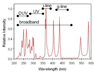
Operators can then select the illumination wavelenght by inserting bandpass filters in the lamphouse: An “i-line” mask-aligner cuts all spectral lines except the 365nm line, while a “broadband” mask-aligner does not filter the light source and, consequently all UV spectral lines are illuminating the substrates and are absorbed by the resist. Potentially, the DUV spectral line can also be used with an appropriate filter if all the optical elements, as well as the mask, are made of quartz.
Direct Laser writer :
Direct laser writing is a maskless lithography (MPL) technology which was initially developped in 1995 at the Microelectronics and Computer Technology Corporation (MCC) in Austin, Texas. In a direct laser writer, a DUV or UV laser is directly focussed into a very small focal spot (< 500nm) on the substrate without passing through a mask. The substrate moves under the objective lens and the laser replicates the layout by exposing only the digitized area. The stage movement can be either: 1) rasterized (line by line), which is faster, more accurate but with possible stripe overlap (“stitching”) defects; 2) vectorized, which is slower but can result in stitching-free exposure.
Furthermore, in the latest generation of direct laser writing equipment, multiple laser beams are used, combined with the used of 1D or 2D micro-arrays of spatial light modulating (SLMs) to no-longer expose a single spot on the substrate, but a projected image of the SLM device, greatly enhancing the througput of the equipment.
Due to their flexibility, ease of use and cost-effectiveness, direct laser writers are very popular in research and development (R&D) facilities, when processing is limited to small batch production.
In production facilities however, they are still limited in terms of througput and suffer from data handling issues with large polygon-count layouts, i.e. when structuring 300mm diameter wafers with a high density of high resolution patterns. Due to this, their use is mainly limited to mask/reticle writing equipment where critical dimension, throughput, and rapid data handling are less of an issue.
Stepper :
The stepper is an exposure system, dedicated to production (>100 wafers/hour), that evolve from the mask-aligner. In opposition to the latter, there is no contact/proximity between the wafer and the mask (reticle), but a projection lense is interposed between them in order to reduce the size of the image of the reticle (usually by a factor of 4x or 5x) onto the wafer, greatly improving the resolution potential of the equipment. Usually, one shot through the reticle will only expose a small fraction of the wafer, called the “field”. By stepping the exposure stage and repeating this process, full wafer coverage is obtained.
The first generation of stepper systems were using i-line (365nm) illumination from Hg lamps and were capable to print down to a critical dimension (CD) of ~350nm, while the latest generation are using a KrF excimer laser emitting at 248nm, and are capable to reach down to ~110nm.
The first commercial stepper was developed in 1975, by the Geophysics Corporation of America (GCA) company and was rapidly sold to all the main chipmakers of the time, including IBM, ATT, and Fairchild.
In the early 1980’s, the Japanese semiconductor industry (Fujitsu, Hitachi, Mitsubishi, NEC, Toshiba) started to catch up to US companies due to massive government investments into VLSI research projects. As a result of these joint projects, Nikon and Canon started to develop photolithography equipment (both mask-aligners and steppers) and rapidly took over the market from US companies.
Finally, the third major supplier of stepper systems, ASML, was founded in 1985 from a joint venture of Philips and ASM.
Scanner :
As the critical dimension (CD) of devices continued to scale down, new innovations were needed in order to push the printing resolution of photolithography systems. The CD of a photolithography system is usually described by the Rayleigh criterion equation :
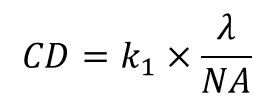
NA is the numerical aperture of the optical system, λ is the illumination wavelength and k1 a process-related parameter, which includes the effect of the resist chemistry (PEB, chemical amplification,…), the mask technology (phase-shift masks, OPC,…), and the exposure conditions (off-axis, double patterning, …).
The first DUV scanner was launched in 1995 by Nikon. In a scanner, both the reticle and the wafer stage are moving together, in synchronized opposite directions during the exposure shot. This way, only a small fraction of the lens (the central part) is used. This allowed to greatly increase the numerical aperture of the optical system.
From 1998, thanks to the development of a new generation of photoresist with absorbtion tailored at 193nm, ArF excimer lasers started to replace KrF lasers as scanner illumination source.
In 2004, ASML introduced the first ArF immersion scanner, and Nikon launched their own comparable tool one year later. In an immersion scanner, water is introduced as an immersion media between the lens and the photoresist. This lead to a new large increase in the numerical aparture of the lens from a theoretical limit of NA = 1 with air as immersion medium to about NA = 1.33 with water.
In 2013, ASML introduced the first extreme UV (EUV) scanner, using a laser-pulsed tin (Sn) plasma light source emitting at 13.5 nm. Lenses are replaced by reflective mirrors in a vacuum environment since no material, even air, stays transparent at this wavelength. ASML is currently the only supplier of EUV lithography equipment.
To illuminate the photoresist selectively through a mask/reticle or directly with a laser.
After exposure, the photoresist (PR) needs to be developed. The development is critical to determine the shape of the PR profile and controlling linewidth.
Post exposure bake
Prior to the development, some photoresists (mainly negative resists and chemically amplified resists) will require a post-exposure bake (PEB) to fully complete the photoreaction and transform the PR into a soluble or insoluble compound.
Another positive aspect of PEB is that it improves the quality of the resist sidewalls (reduction of standing waves, better line edge roughness (LER), due to the diffusion of the photoactive compound in the base polymer.
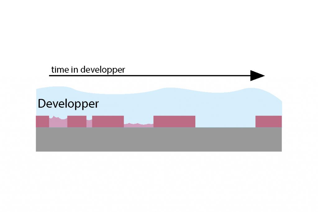
Development
Most developpers are from an aqueous base solution with tetramethyl ammonium hydroxide (TMAH), potassium hydroxide (KOH), or sodium hydroxide (NaOH). Since the last two contains metallic ions (K+, Na+), they might not be compatible with micro-electronic applications.
For standard-size SEMI wafers (4 and 6 inch), it is possible to use the automatic development tools. In this case, two development techniques are possible (illustrated below) :
- Puddle: the wafer is static with a layer of developper covering the whole surface
- Spray: the wafer is rotating and the developer is sprayed onto it
For both techniques, the developper is rinsed by rotating the wafer at high speed and dispensing deionized (DI) water onto it.

When performed manually, the development will consist in imerging the exposed substrate into the developper solution for the appropriate time and using deionized water to rinse it.
Users should consider the following important information:
- Substrate compatibility: Most TMAH and KOH-based developers attack alkaline-sensitive materials, such as aluminium or copper. Alternative photoresist developers are available for manual development to minimize aluminium etching.
- Developer selectivity and dark erosion: The photoresist development rate will strongly depend on the developer concentration, which is optimized to achieve a reasonably fast development rate (typically around 2μm/min) while minimising the erosion of unexposed resist region (dark erosion). Still the selectivity of the developer is not infinite and the PR thickness will be reduced during the development step by ~10%.
- Developer exhaustion: In the case of manual immersion development, the photoresist development rate will slowly decrease: 1) Over time due to the absorption of CO2 from the ambiant air that reduces the activity of the developer; 2) For each consecutive wafer, especially with thick photoresist and large cleared surfaces, due to the saturation of the developer solution with dissolution byproducts. A refresh of the developer might be needed after a certain duration / number of wafers.
To dissolve the photoresist selectively in the developer solution.
Following the development step, additional thermal treatments can be performed on the photoresist:
Hardbake
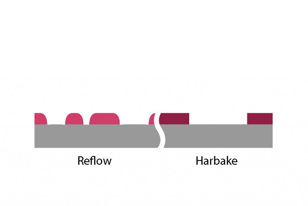
To increase the photoresist stability for certain application, it is possible to further bake the developped photoresist, for a longer duration than applied during the softbake. The hardbake have various effect but mainly : 1) a reduction of the remaining PR solvent concentration, 2) a reduction in the DNQ PR concentration, 3) an increase in the degree of crosslinking.
The hardbake can help in improving the resist adhesion to the substrate, improving the chemical stability to certain wet etching processes (alkaline wet etching, electro-plating with pH > 7), as well as certain dry etching plasma compositions.
The use of a hardbake step should be carefully evaluated, and its parameters optimized since it also has potential drawbacks: The hardbake step, by reducing the solvent content in the resist can make it more brittle and more difficult to be stripped.
Reflow
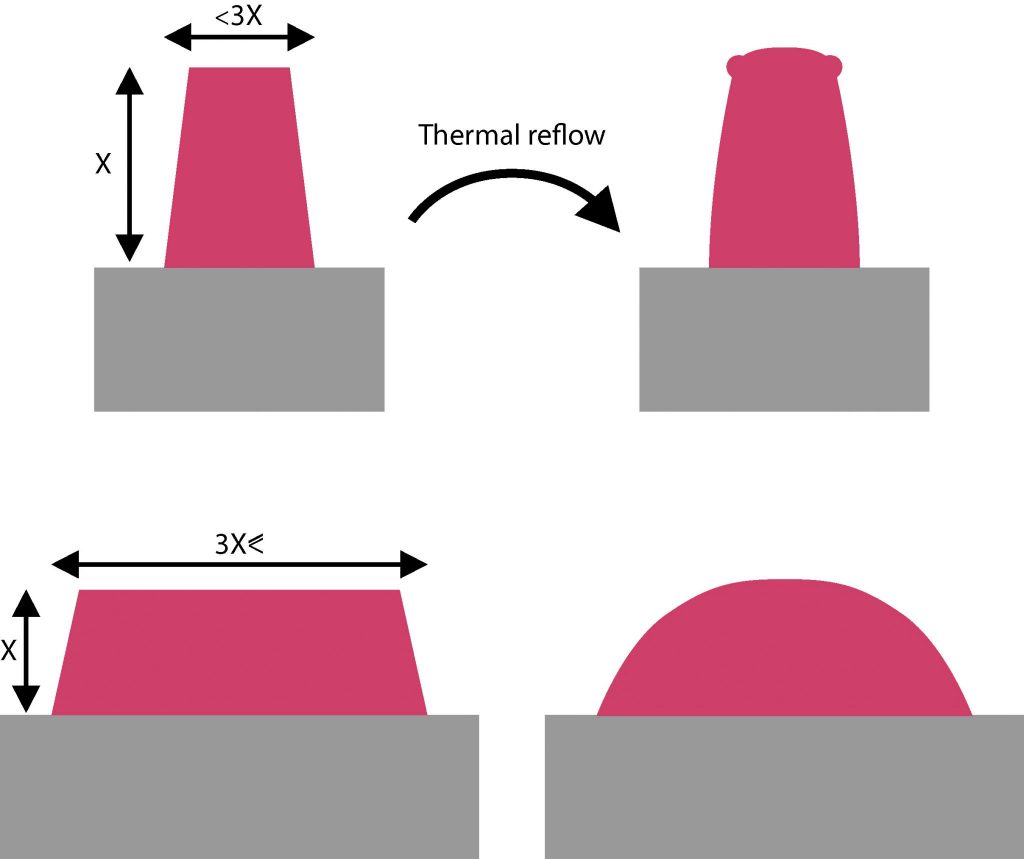
In addition to the above effects, positive photoresist that are heated above their softening point (anywhere from 110°C to 130°C depending on the resist) will start to reflow. The resist profile is modified and rounded (sidewalls are less vertical) in order to decrease its surface energy. A reflow treatment can be recommended in combination with certain etching processes such as physical argon ion beam etching, to prevent redeposition of material on the PR sidewalls
Furthermore, reshaping the resist profile has been used in many microfabrication processes to obtain spheres or tilted profiles, and then transferred to the underlying substrate, to use as micro-optics components.
Dimensions of the design and reflow process parameters (i.e. duration and temperature) have both, in addition to the intrinsic properties of the resist, an extensive impact on the final resist profile.
The overall volume of the photoresist shrinks only a little during the reflow, also one must take into account dimensional restrictions. To round the square shapes of sidewalls, there must be enough area where the photresist can flow to. Typically, a width 3 times larger that the height as illustrated below.
To shape and increase the chemical stability of the photoresist
Photolithography being generally only used as a temporary masking process, a proper way to remove the resist is needed. The two main methods are :
Wet chemistry
The cross-linking degree of the photoresist has a major impact on its solubility. Positive photoresist tends to be higly soluble. Crosslinking being an inherent part of negative ones, they show a lower solubility and are generally slightly more difficult to strip.
- Solvents: Solvents are the go-to option for stripping due to their compatibility to most substrates. However, users should be aware that some transitions metals (in particular Ni, Cu, Co, In, Al, Fe, Ti, Zn) can be oxidized/corroded by strong solvents under specific conditions.
- Acetone – Not ideal because of its high volatility.
- N-methylpyrrolidone (NMP) – It has been the standard for many years but is slowly phased out after having been classified as toxic (organ and reproductive toxicity).
- Dimethyl sulfoxide (DMSO) – An alternative to NMP which show comparable dissolution results and is not classified as toxic.
- N-ethyl pyrrolidone (NEP) – Used in certain stripping formulations and a little bit less hazardous than NMP according to most classifications.
- Bases: Alkaline solutions, including the standard PR developers (with lesser dilution), can be an alternative to solvent stripping in specific cases (e.g. for thick negative resist, after dry etching, etc..). However, metals and even crystaline silicon can be attacked by high pH solutions.
- Acids: Strong acids such as sulfuric acid, nitric acid, aqua regia, piranha can also be used to remove photoresists. This is used in last resort when safer alternatives are not working, or not possible for compatibility reasons.
Plasma asher (O2)
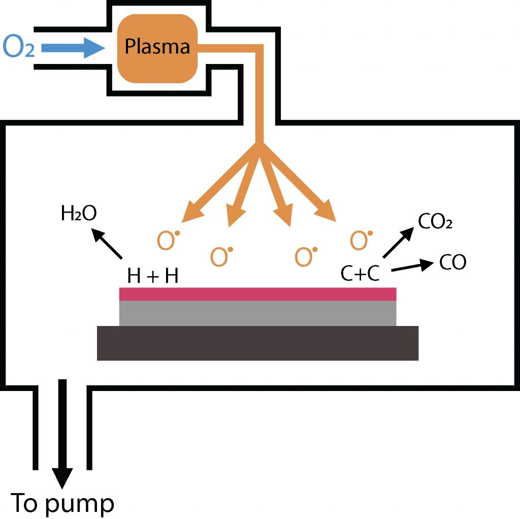
Molecular oxygen gas is introduced into a plasma chamber where a microwave plasma is generated under high vacuum conditions. High-energy electrons in the plasma collide with oxygen molecules, providing in some cases enough energy to split them into oxygen radicals.
These oxygen radicals are pumped into the process chamber, where they react with organic hydrocarbon residues, such as photoresists, on the heated substrate surface. The reaction produces volatile compounds like carbon oxides and water, which are then removed by the vacuum system.
To remove the photoresist from the substrate.
