Introduction to BackScattered Electrons
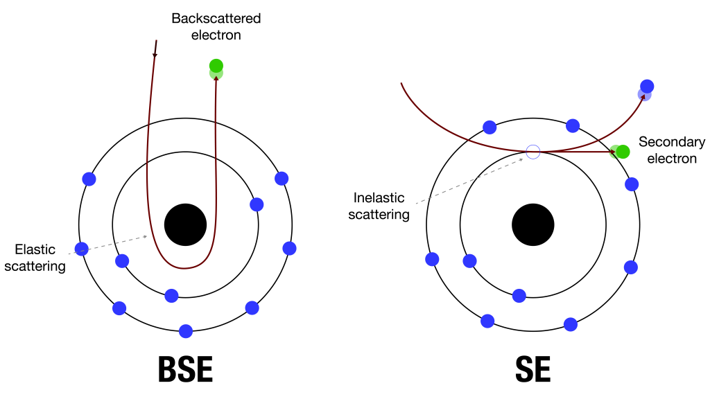
BackScattered electrons (BSE), unlike Secondary Electrons (SE), result from elastic interactions with the sample and are deflected at large angles (greater than 90 degrees) to ultimately exit the specimen.

Indeed, BSE emission consists of primary electrons that, after undergoing a number of elastic collisions with atomic nuclei and inelastic collisions with orbital electrons, return to the surface and emerge from the target, not necessarily at the same location with an energy more or less close to incident electron energy (E0). The energy spectrum of electrons displays the arbitrary boundary set at 50 eV between secondary and backscattered electrons.

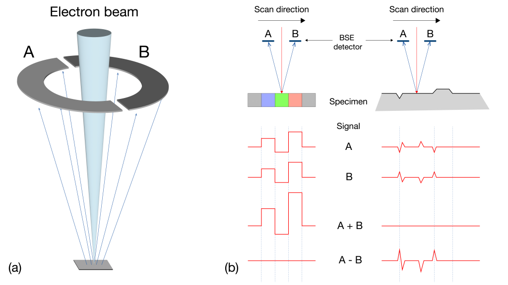
Once outside in the vacuum, these electrons can be captured by a detector to create an image known as a backscattered electron image. This type of electrons is known to naturally exhibit compositional contrast images since these electrons are strongly sensitive to the atomic density (atomic number Z) of the specimen material. However, some detectors (semiconductor-based) divided into several independent detection cells enable the achievement of topographic contrast, particularly due to the sensitive variation in BSE emission based on their angular distribution. The angular Backscatter Electron Detector (aBSD) is used to detect backscattered electrons, that have been scattered at very low angles.

The SEM Zeiss Crossbeam has a dedicated backscattered electron detector of this type. This new detector is only available on this microscope.
How to operate the aBSD detector
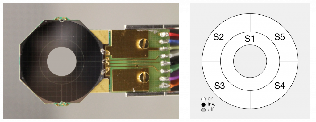
This new detector contains five input channels:
- The inner ring is especially used to image the material contrast as it has a high take-off angle.
- The outer ring is divided into four segments to explore the topographic contrast with different illumination.

The aBSD detector is a pneumatically retractable annular backscattered electron detector.
Preliminary. Initially, to facilitate the following steps, it is necessary to use the inLens detector to produce a “classic” image formed from secondary electrons. Ensure a satisfactory image by adjusting the contrast, brightness, focus, aperture, and stigmatization before proceeding.
Although the aBSD detector appears in the dropdown list of available detectors under the “Imaging” tab, it must first be inserted into the chamber since it is retracted at other times to avoid interacting with other detectors.
1. From the Panel Configuration Bar, select “BSD Control”. The BSD Control panel is displayed. As indicated in the position readout, the BSD is initially in the out position (BSD Position = Out).
2. In the BSD Control panel, click “BSD in” button to insert the aBSD detector.
a. The stage is lowered by 20 mm to give space for the detector to be inserted.
b. The detector is inserted. This could be observed on the CCD view.
3. Using the joystick, raise the sample to a working distance (WD) of 5mm to 12mm from the aBSD detector, which is now at the height of the pole piece endcap.
When inserted, the aBSD detector is positioned directly underneath the objective lens. The lower edge of the detector is then located at a working distance of 1.5 mm. If you move the specimen to a working distance below 1.5 mm, then you damage the aBSD detector.
– Do not move the specimen to WD below 2 mm.
– Be careful when you tilt the specimen.
4. In the Crossbeam SEM Control panel, select the Imaging tab.
5. From the Signal A drop-down list, select aBSD1.
6. Select the “BSD:COMPO” mode
7. Select a gain setting between “High” and “Very High”. This step is not mandatory but greatly assists in obtaining a usable signal. All the 5 cells will be acquiring the signal.
8. Adjust the acceleration voltage EHT the current as needed to perceive a signal in
order to optimize the image.
9. In the BSD Control panel, click a quadrant symbol to toggle its status between on (white),
inverted (black), and off (gray).
10. To choose the respective mode, click BSD: COMPO or BSD: TOPO.
The default setting for BSD is BSD: COMPO. All six segments (S1–S6, aBSD) or four segments
(S1–S4, BSD) are set to on and an image that is high in atomic number contrast is
obtained.
The default mode for BSD: TOPO is S3 on, S4 on, S5 inv and S6 inv (aBSD) and S1 on, S2
on, S3 inv and S4 inv (BSD).
11. From the BSD Gain drop-down list, select Low, Medium, High, or Very High.