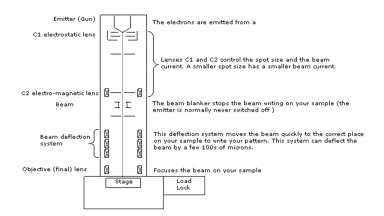
Tool Description
Explanation of basic tool components and concepts, such as writing fields, stitching, dose, frequency, etc.
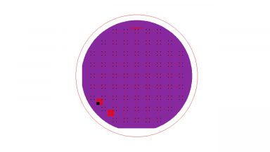
Writing Strategy
Explanation of image formation using a round Gaussian beam spot and rectangular pixel grid. Beam size as a function of beam current.
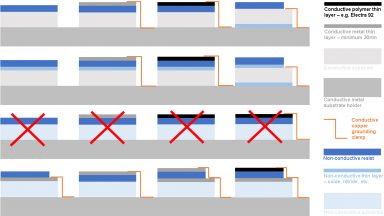
Conductive Substrate
Ebeam litho at 100kV can only be performed on electrically conductive substrates.
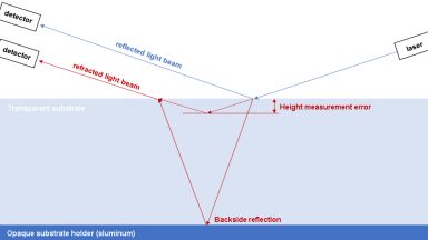
Opaque Reflective Surface
Sample surface must be opaque and reflective to enable correct in-situ laser height measurement during exposure.
Alignment
Written patterns can be aligned to pre-existing structures on the wafers/chips. Overlaying of multiple levels is possible.