When you access EPFL websites, we may set cookies on your devices and process personal data about you in accordance with our privacy policy. You can block cookies by using your browser settings.
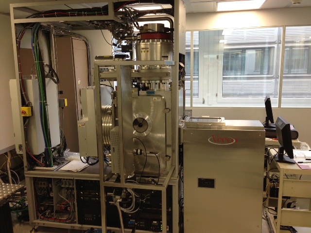
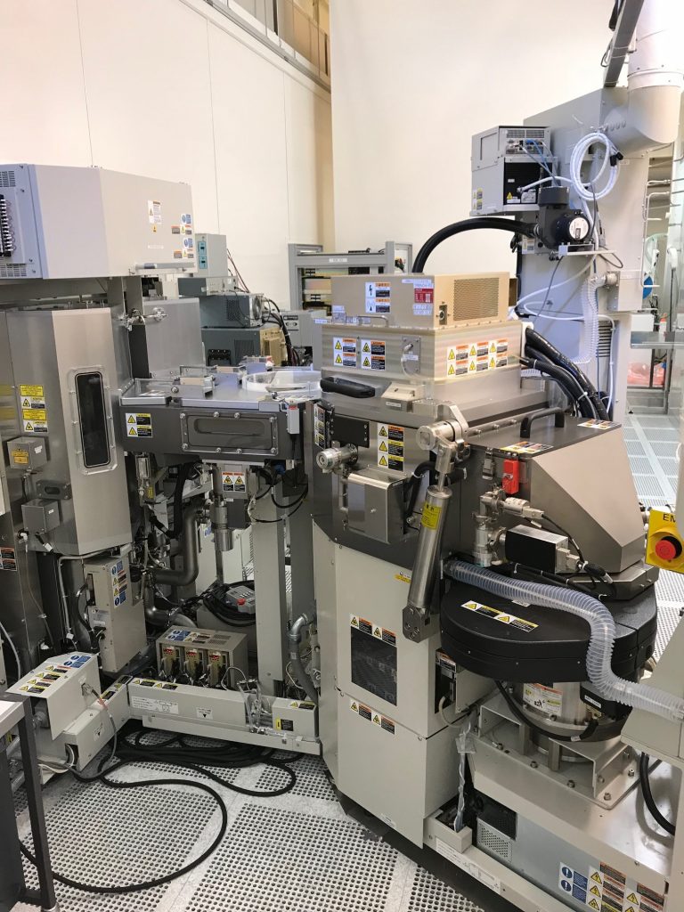
– 100mm wafers (max 4mm thick) – Argon ions 350mm broad-beam – Large range energy capability (50V to 800V) – High uniformity and high collimation – Pure physical sputtering of any material – Low temperature substrate fixture (<90°C) – Secondary Ions Mass Spectroscopy – Location: Zone 11
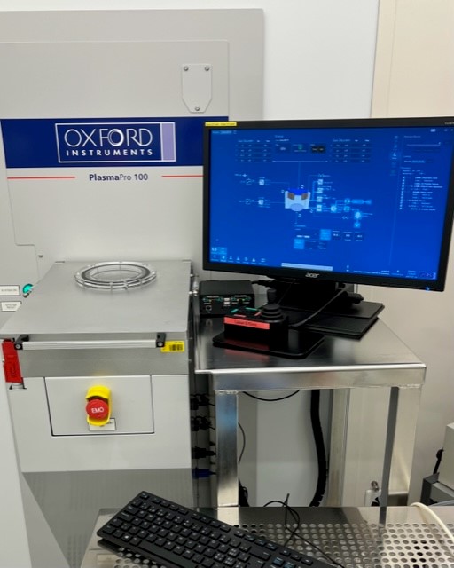
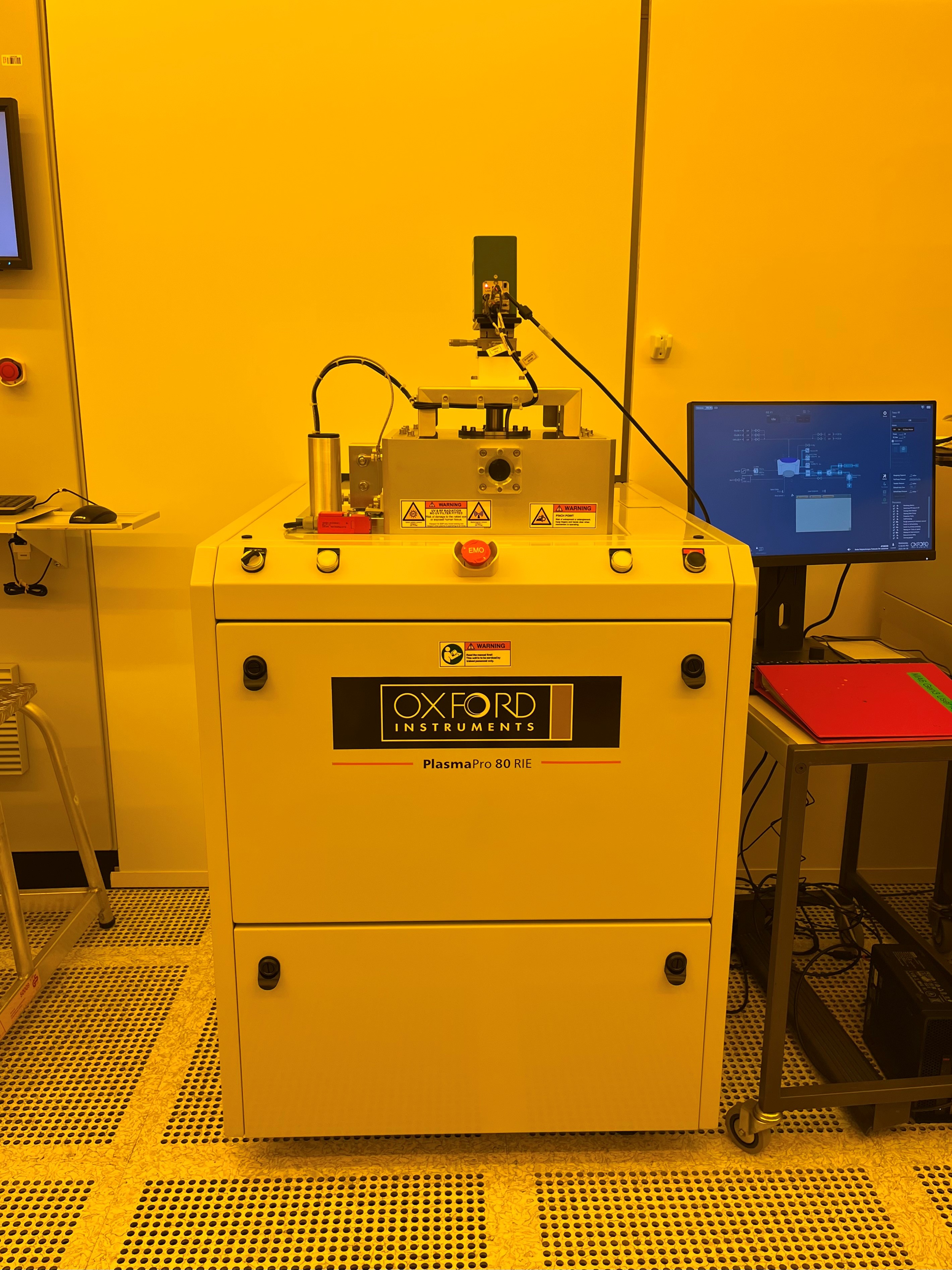
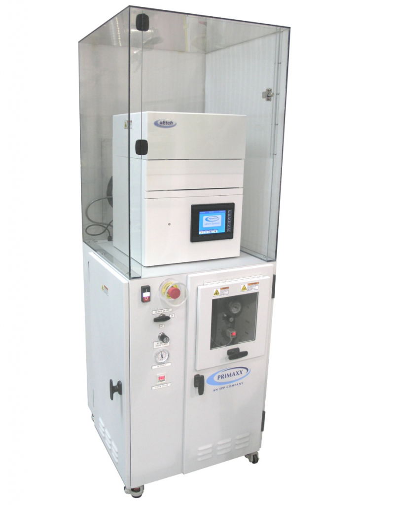
Samples must NOT have presence of any metallics, or traces of metallics (real or suspicion), even buried. – ICP plasma etcher 100mm wafers – Fluorine chemistry – Electrostatic clamping – Microelectronic compatible equipment – SiO2 and Si3N4 thin films etching – Location: Zone 2
Samples must NOT have presence of any metallics, or traces of metallics (real or suspicion), even buried. – DRM (Dipole Ring Magnet) – 100mm – RIE with magnetic field assistance – Fluorine chemistry – Electrostatic clamping – Microelectronic compatible equipment – SiO2 and Si3N4 thin films etching – Location: Zone 2
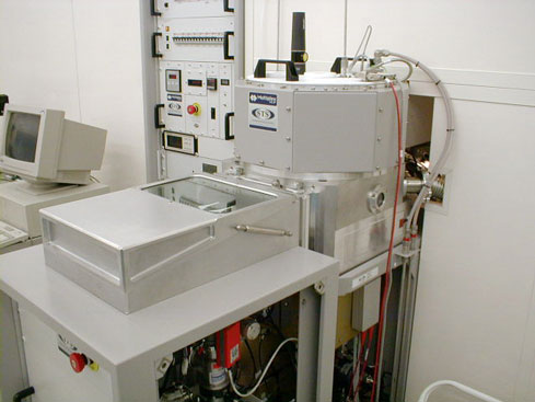
Samples must NOT have presence of any metallics, or traces of metallics (real or suspicion), even buried. – RIE plasma etcher – CHF3, SF6, O2, Ar – Max 300W @ 13.56MHz – Open-load system (no load lock) – Chips to wafer up to 200mm – hBN, SiGe, Graphite and Graphene soft etching – Location: Zone 3
The tool is currently being installed, not yet operational – RIE plasma etcher – CF4, CHF3, SF6, O2, Ar – Max 300W @ 13.56MHz – Open-load system (no load lock) – Chips to wafer up to 200mm – Nb, Ta and superconducting nitride thin-films etching – Location: Zone 6
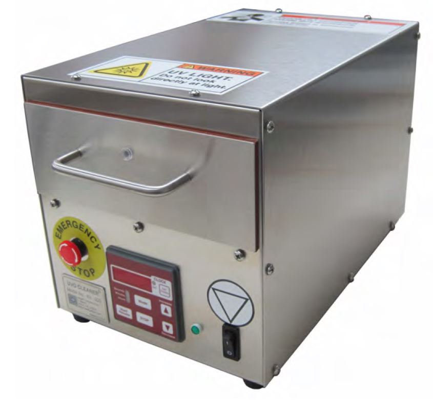
– 8 inches wafers to piece parts – HF chemistry – SiO2 etch – Controllable etch rate (nm/min to um/min) – Dry process without sticking issues – Location: Zone 2
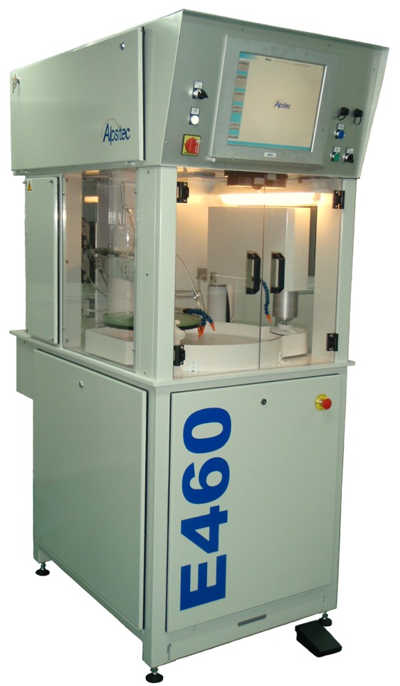
– Post CMP Cleaning of 4”, 6” and 8” wafers – Metal contaminated wafers can be processed with dedicated brushes, please contact staff – Location: Zone 18/19
– Silicon, III/V materials and glass types grinding – Single wafers, stacked wafers and chips (from a few mm2 to full 8″ wafers) – Frame mounting on UV-tape – Disco DCS1440 atomizing cleaning – Roughness < 100nm, TTV ~ 1micron – Location: Zone 22
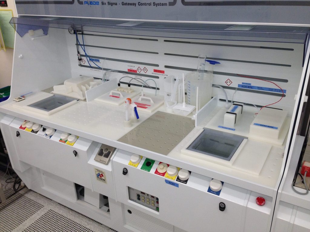
– 100, 150 mm wafers and piece parts – 100 mm chuck to protect wafer back side – KOH chemistry 40%/60°C – Silicon anisotropic etch – Location: Zone 18/19