Restrictions and Precautions
RESERVATION RULES AND BOOKING FEES POLICY:
1. Maximum allowed booking per person between 9am and 5pm is 2 hours. It is still possible to get 4 consecutive hours from 7am to 11am or from 3pm to 7pm.
2. Reservation names must correspond to operators.
1. Maximum allowed booking per person between 9am and 5pm is 2 hours. It is still possible to get 4 consecutive hours from 7am to 11am or from 3pm to 7pm.
2. Reservation names must correspond to operators.
Contents:
I. Introduction ↑
SPTS Advanced Plasma System (APS) module is an ICP-based high density plasma source. This system was optimized for etching dielectrics (e.g. SiO2, SixNy, SiC, Al2O3, glass types…) which are usually difficult to etch using conventional RIE or ICP sources.
Main features of the system are:
- High density plasma source
- Wafer voltage biasing independent from the ICP
- Electrostatic clamping => no EBR required
- Powerful gas process pumping arrangement
- Loadlock/chamber transfers for single wafer processing
- Control software offering fully automated processes
- End-point detection system (optical spectroscopy)
Gases availables:
- O2 [0 – 100 sccm].
- Ar [0 – 100 sccm].
- CHF3 [0 – 100 sccm].
- He [0 – 500 sccm].
- C4F8 [0 – 100 sccm].
- SF6 [0 – 100 sccm] & [0 – 500 sccm].
- H2 [0 – 50 sccm].
II. Processes available ↑
On the SPTS etcher, a process is defined as a sequence of several steps:
- Wafer is loaded in, clamped and helium back cooling is switched-on.
- Wafer cooling condition is checked by a leak-up-rate (LUR): the chamber is isolated from the pumping system and increase of pressure inside the chamber is recorded. This pressure increase is due to helium leaking in between the chuck and the clamped wafer. To ensure correct cooling of the wafer during etching, LUR should not exceed 200mtorr/min.
- Wafer is etched with possibility of End-Point Detection (EPD) monitoring. EPD system is used in “monitoring only” mode and therefore it does not control the process chamber. If no action is done by the operator to manually stop the etching, the process will run until the set time has elapsed, even if an end point is detected by the EPD system.
- Dechuck step: electrostatic clamping is switched-off and a low power argon plasma runs for few seconds to help remove accumulated charges that may remain. No chuck biasing is applied here to ensure no sample damage by argon ions.
- The wafer is unloaded and, if necessary, an automatic cleaning of both the chamber and the chuck starts, stopping automatically upon end-point detection.
- Machine is ready for another run.
| Material DUV42P BARC from Brewer | SH temp (°C) 10 | Process name BARC_Slow | Chemistry CHF3/O2 | Mask material JSR M108Y JSR M35G | Etch rate (nm/min) DUV42P: 80 M108Y, M35G: 100 Si: 120 SiO2: 215 | Selectivity/mask <1:1 |
| Material Si3N4 | SH temp (°C) 10 | Process name Si3N4_Smooth | Chemistry CHF3/SF6 | Mask material ZEP/CSAR PR | Etch rate (nm/min) Si3N4: 160 to 220 Si: 235 WetOx: 165 Nb: 150 PR: 70 | Selectivity/mask 2:1 |
| Material SiO2, Si3N4 | SH temp (°C) 10 | Process name SiO2_PR_1:1 | Chemistry CHF3/He | Mask material PR | Etch rate (nm/min) WetOx: 230 Si3N4: 200 SiN LS: 185 Si: 95 TiO2:40 | Selectivity/mask 1.7:1 |
| Material SiO2, Si3N4 | SH temp (°C) 10 | Process name SiO2_PR_2:1 | Chemistry C4F8/He | Mask material PR | Etch rate (nm/min) WetOx: 440 Si3N4: 110 SiN LS: 95 Si: 50 | Selectivity/mask 2.8:1 |
| Material SiO2, Si3N4 | SH temp (°C) 10 | Process name SiO2_PR_3:1 | Chemistry C4F8/H2/He | Mask material PR ZEP/CSAR | Etch rate (nm/min) WetOx: 380 Si3N4: 255 SiN LS: 190 Si: 35 ZEP / CSAR: 130 | Selectivity/mask 4.2:1 |
| Material SiO2, Si3N4 | SH temp (°C) 10 | Process name SiO2_PR_3:1_SOFT | Chemistry C4F8/He | Mask material PR | Etch rate (nm/min) WetOx: 320 Si3N4: 70 SiN LS: 60 Si: 35 | Selectivity/mask 3.7:1 |
| Material SiO2, Si3N4 | SH temp (°C) 10 | Process name SiO2_PR_5:1 | Chemistry C4F8/H2/He | Mask material PR | Etch rate (nm/min) WetOx: 235 Si3N4: 255 SiN LS: 235 Si: 25 | Selectivity/mask 6.5:1 |
| Material SiO2, Si3N4 | SH temp (°C) 10 | Process name SiO2_PR_soft | Chemistry C4F8/H2/He | Mask material PR | Etch rate (nm/min) WetOx: 170 | Selectivity/mask >25:1 |
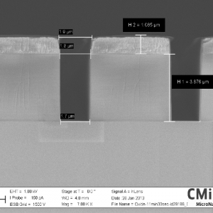
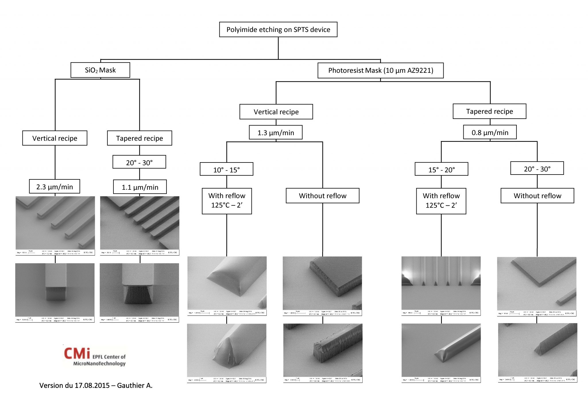
| Material Polyimide | SH temp (°C) 10 | Process name Pi_vertical | Chemistry O2 | Mask material PR SiO2 | Etch rate (nm/min) PI (PR) : 1300 PI (SiO2) : 2300 | Selectivity/mask 1:1 (PR) |
| Material Polyimide | SH temp (°C) 10 | Process name Pi_tapered | Chemistry O2 | Mask material PR SiO2 | Etch rate (nm/min) PI (PR) : 800 PI (SiO2) : 1100 | Selectivity/mask 1:1 (PR) |
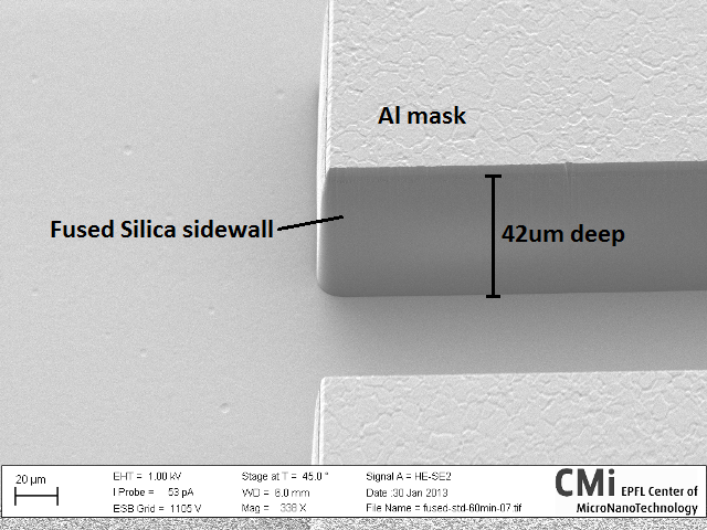
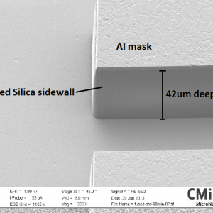
| Material Fused Silica | SH temp (°C) 20 | Process name Fused_silica | Chemistry C4F8/O2 | Mask material Al | Etch rate (nm/min) 760 | Selectivity/mask >12:1 |
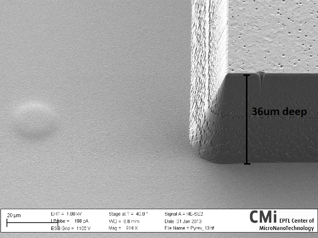
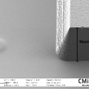
| Material Pyrex | SH temp (°C) 25 | Process name Pyrex | Chemistry C4F8/O2 | Mask material Al Cr or Ni | Etch rate (nm/min) 580 | Selectivity/mask 8:1 20:1 |
| Material LiNbO3 | SH temp (°C) -10 | Process name LiNbO3_wafers | Chemistry CHF3/Ar | Mask material Cr | Etch rate (nm/min) 90 | Selectivity/mask 4:1 |
| Material Chamber clean | SH temp (°C) — | Process name O2 clean with wafer | Chemistry O2 | Mask material — | Etch rate (nm/min) — | Selectivity/mask — |
Clearing the PR mask after Si3N4 and SiO2 etch requires both dry and wet treatments:
- Start with an oxygen plasma using the Tepla GiGAbatch or the ESI3511.
- Then do a wet remover treatment using the Ultrafab wetbench.
- If necessary, remove final residues with the Tepla GiGAbatch or the ESI3511 again.
- If DUV resist on BARC was used as a mask, a 30sec dip in HF1% helps clear residues left from BARC layer
III. Modus Operandi ↑
- System is in idle mode by default: no wafer is loaded, CTC software is open (if not open it), loadlock is under vacuum.
- First login in the CTC software: Select the account “other”, and enter : 1 (for the account) 1 (for the password).
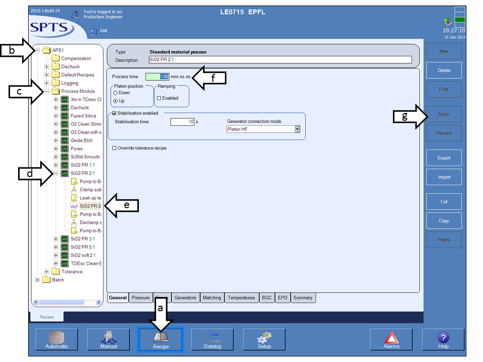
- Select:
- (a) Recipe,
- (b) APS1 (hit the cross),
- (c) Process Module (hit the cross),
- (d) The process you are interested in (hit the cross),
- (e) The etching step (SiO2_PR_2:1 in the example)
- (f) Process parameters are visible, you can only modify the process time in General
- (g) Save the change (hit Apply on the right)
- Select the “Automatic” mode, “Vent” the load lock, and load the wafer on the loading arm.

- Select a batch recipe in the predefined batch recipes list.
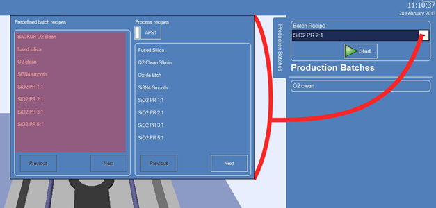
- Click on “Start” icon and check that the batch uses the correct recipe. Then click “Next” and finally “Start”. This loads the wafer inside the process module and starts automatically the etching sequence detailed previously.
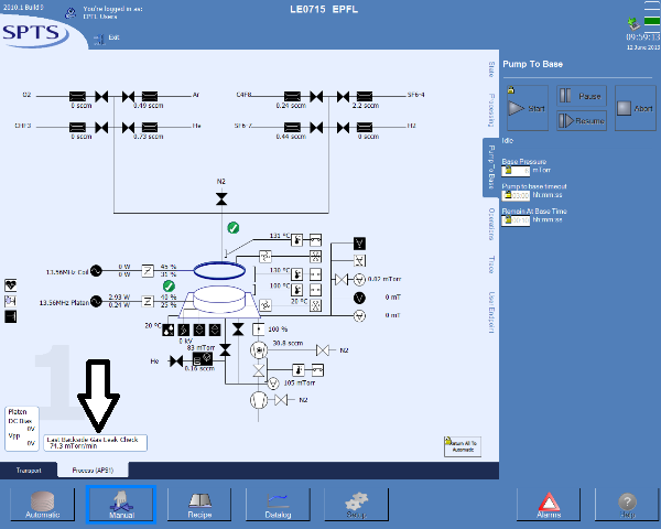
- Select the “Manual” mode and click onto “Process (APS1)”. Check the LUR test and write-down its value in the follow-up file of SPTS etcher available on the table.
- If no action is done by the operator to manually stop the etching, the process will run until the set time has elapsed.
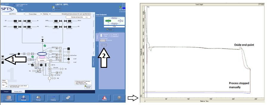
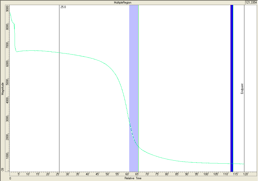
If the etching has to be stopped before the set time, i.e. after end-point is detected, proceed as follows:- Be sure “Manual” control and “Process (APS1)” are active:

-
- Activate the end-point tab and click “Endpoint”:

-
- The Oxide EPD recipe follows the intensity of the 440nm spectral line which corresponds to SiF (etching by-product)
- Then, the system runs the dechuck step, unloads the wafer, vents the loadlock and runs the automatic cleaning of both chamber and chuck (if applicable).
- Load the next wafer to be etched or if you are done pump the load lock.

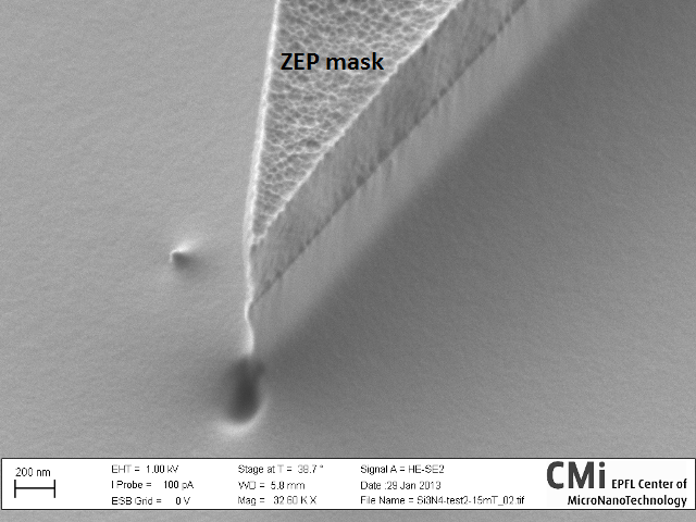
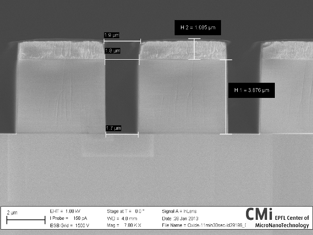
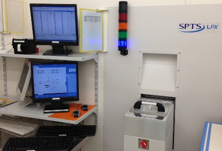
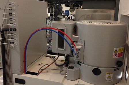
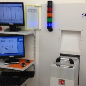
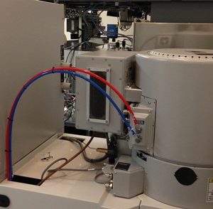
IV. Photo gallery ↑