AFM
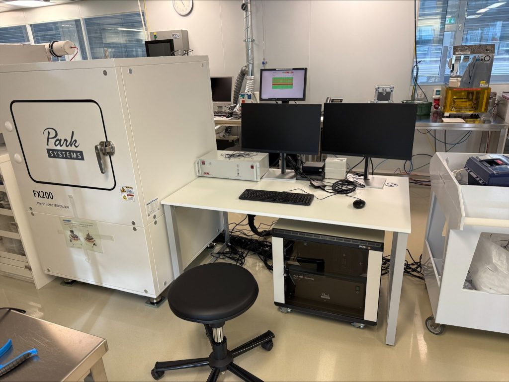
- Equipement
- – Sample chuck for up to 200mm wafers
– Small sample holder supports samples of arbitrary shape up to 10 mm x 10 mm
– Automated probe exchanger (16 probe loading slots)
– Automated SLD (Super Luminescence Diode) beam alignment
– Automated sample navigation and measurement for ease-of-use
– XY scan range : 100 um x 100 um typical
– Z scan range : 15 um
– Ultra low noise floor (<0.5 A)
– Distortion free image (<2 nm) with separated XY scanner from Z scanner
– Direct On-Axis Optics with High-Resolution CCD and Integrated LED Illumination
– Macro Optics for 200 mm Sample Overview
– Location: Zone 11 - Documentation
- – Manual
- Responsibles
- D. Bouvet
A. Toros
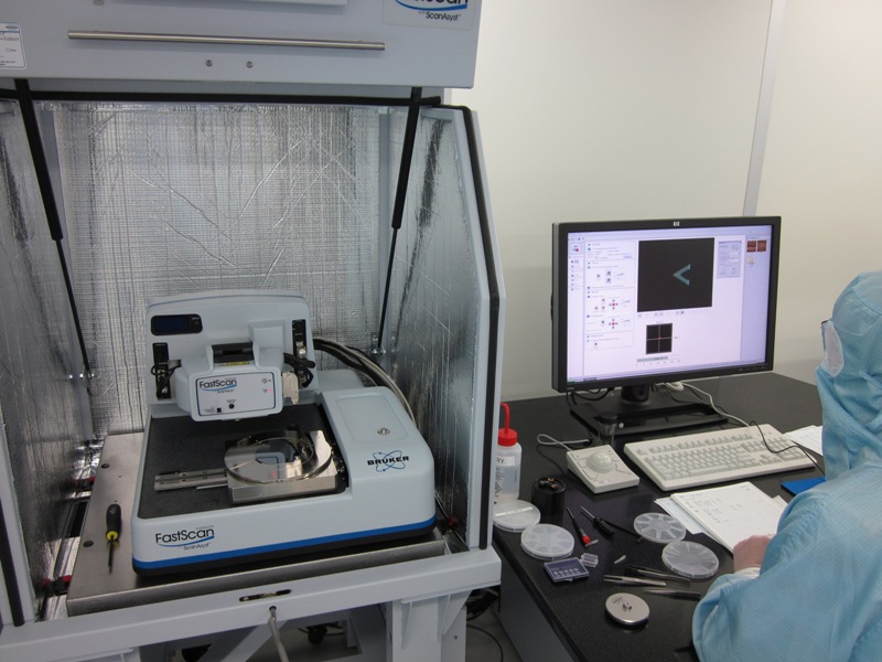
- Equipement
- – 150mm X 180mm inspectable area with rotating chuck
– Automated laser and detector alignment
– <30pm vertical noise with closed-loop Icon scanner
– High speed imaging with FastScan scanner
– Location: Zone 15 - Documentation
- – Manual
– NEW VERSION (08.05.2025) : User manual - Responsibles
- D. Bouvet
A. Toros
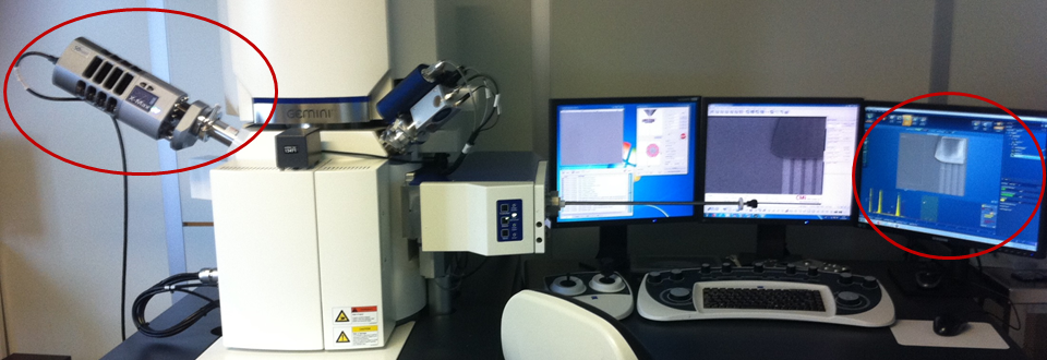
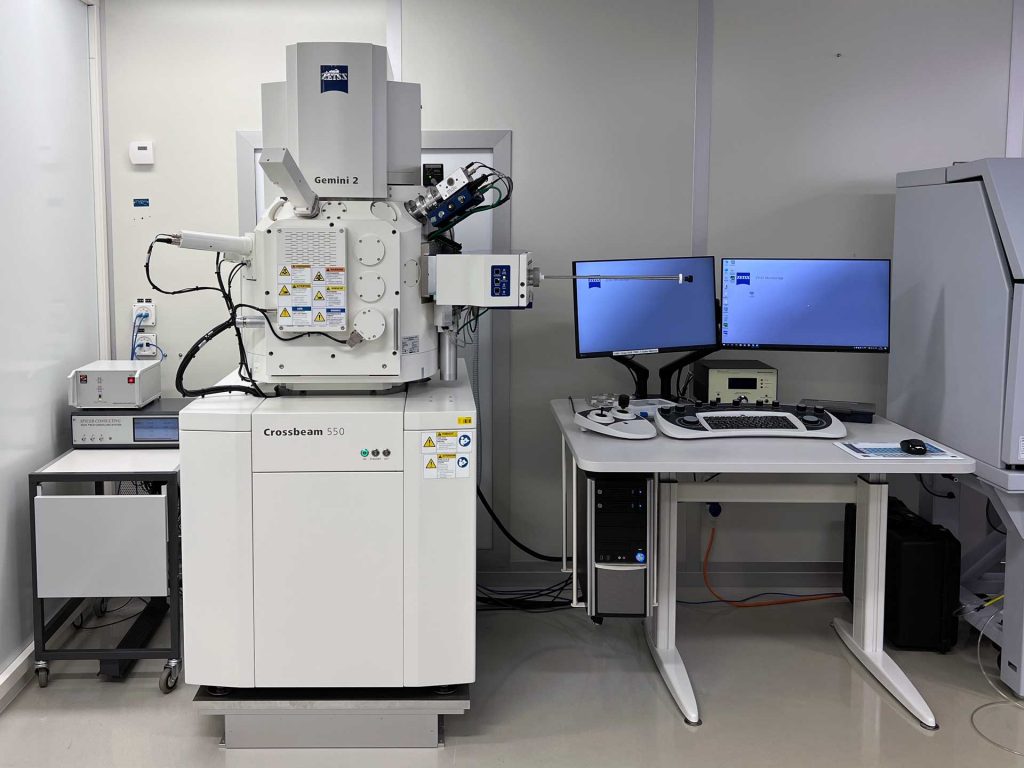
FIB / SEM / EDX / ProSEM
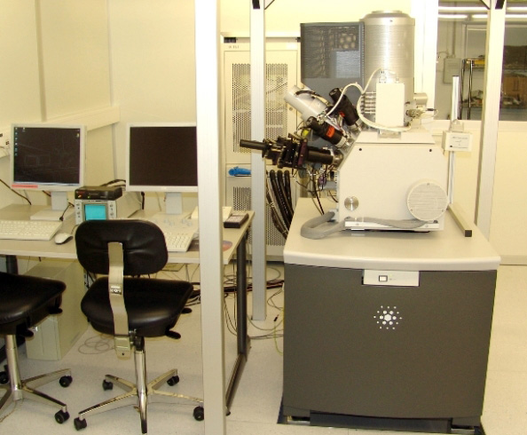
- Equipement
- – 100, 150 mm wafers and piece parts
– High resolution SEM imaging
– Ion beam patterning (> 100nm)
– Up to 30 kV SEM and FIB acceleration voltages
– Cross-sections, TEM lamellas, Omniprobe manipulator
– Location: Zone 8 - Documentation
- – Manual
- Responsibles
- Z. Benes
J. Pernollet
- Equipement
- – Energy Dispersive X-ray Spectroscopy
– Oxford Instruments X-MAX silicon drift type detector 50mm2
– Resolution 127eV FWHM
– Detection limit about 1 atomic %
– AZtec and INCA software
– Location: Zone 15 - Documentation
- – Manual
- Responsibles
- Z. Benes
J. Pernollet
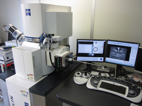
- Equipement
- – 6 & 5 inch masks; 8, 6 & 4 inch wafers, cleaved samples (wafer section) and piece parts
– High resolution SEM imaging (<1nm)
– From 0.02 to 30 kV acceleration voltage
– Detectors: SE, In-Lens, EsB, aBSD and VPSE
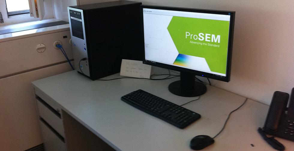
– Additional softwares: SmartStitch, 3DSM, ProSEM, InSPEC
– Location: Zone 15 - Documentation
- – Manual
- Responsibles
- M. Chahid
Z. Benes
- Equipement
- – GenISysSEM image analysis software
– CD and line-edge roughness measurements
– Automatic pattern edge detection
– Multiple features in a single image analysis
– Batch processing of multiple images
– Location: BM1132 - Documentation
- – Manual
- Responsibles
- Z. Benes
J. Pernollet
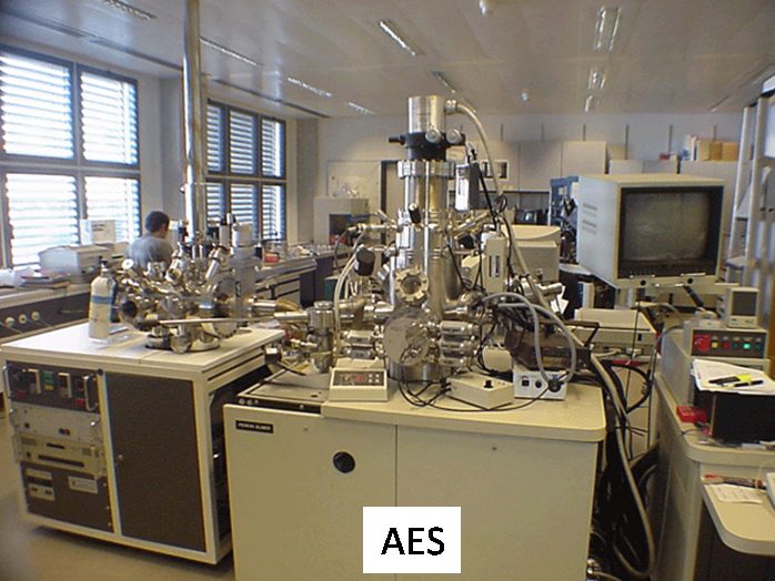
XPS / AES available at MHMC
Please visit “Surface characterization” MHMC page for more details.
Please visit “Surface characterization” MHMC page for more details.
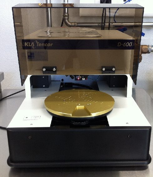
Mechanical profilometers
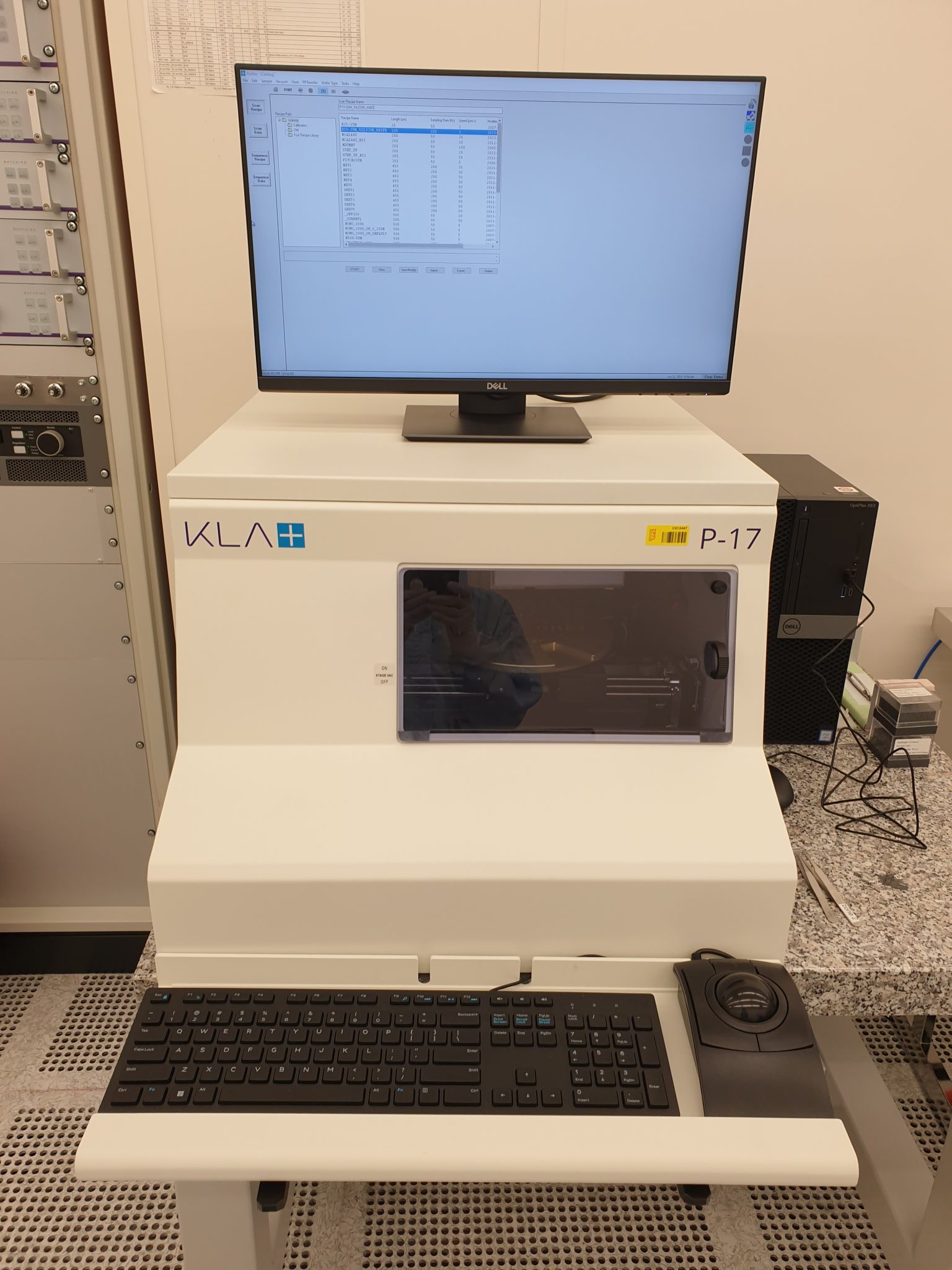
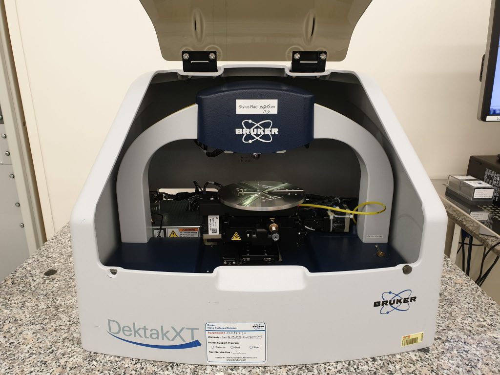
- Equipement
- – Measurement range in Z : up to 1mm
– Step height repeatability: 5A
– 3D stress and 3D mapping
– Location: Zone 15 - Documentation
- – Manual
– Tutorial for database - Responsibles
- D. Bouvet
A. Toros
Optical measurement
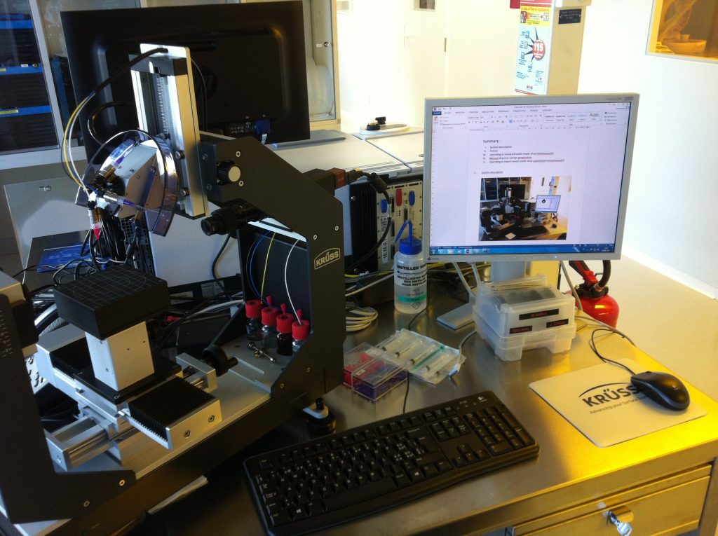
- Equipement
- – Contact Angle and Surface Free Energy (SFE) measurements
– Multi-dosing system (4 automatic and 1 manual syringes)
– Motor-controlled y– axis for multi-drop experiments
– Droplet volume < 5 µl
– Location: Zone 16 - Documentation
- – Equipment Description
– User Manual - Responsibles
- J. Dorsaz
N. Piacentini
M. Pillon
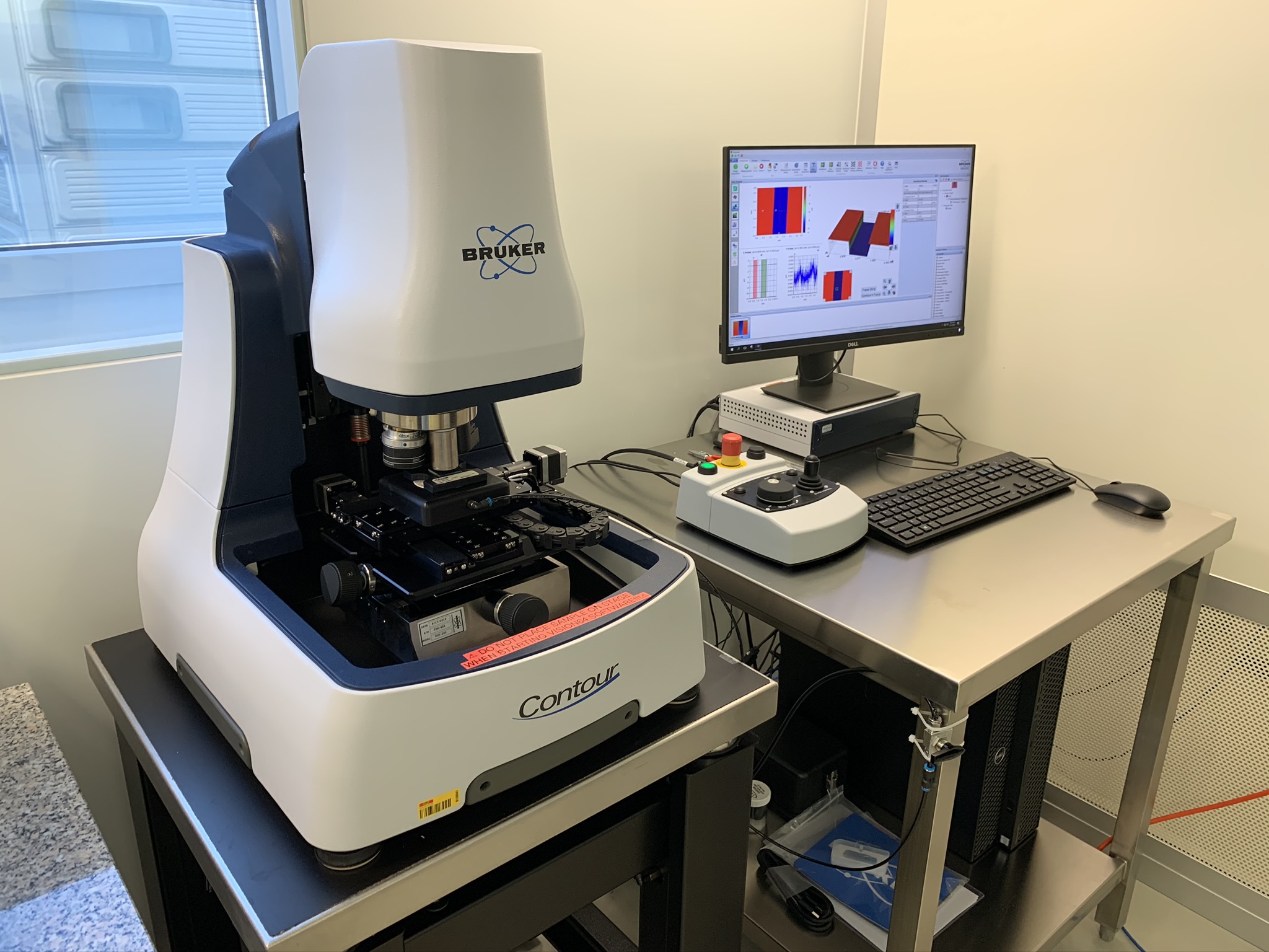
- Equipement
- – Phase shifting interferometry (PSI) for roughness and small steps (< 135 nm)
– Vertical scanning interferometry (VSI) for rough surface and steps up to 10 mm high
– PSI vertical resolution : <0.01 nm
– VSI vertical resolution : <0.75 %
– Spacial resolution : 0.38 µm
– Location: Zone 15 - Documentation
- – Manual
- Responsibles
- C. Hibert
A. Toros
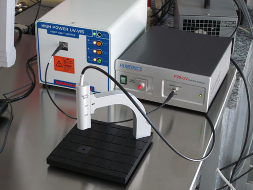
- Equipement
- – Thickness measurement
– Thickness range : 1nm to 40µm
– Thickness and n and k measurement
– Thickness range : 50nm and up
– Wavelength range : 200nm – 1100nm
– Spot size : 1.5mm
– Measurement of Single layers
– Measurement of Multilayer stacks
– Location: Zone 11 - Documentation
- – Manual
- Responsibles
- J. Dorsaz
N. Piacentini
M. Pillon

- Equipement
- – Measurement range : 4nm up to 35µm
– Spatial resolution : 33µm (500um aperture)
– Mono, bi-layers and tri-layer stack measurements
– Location: Zone 3 & Zone 19 - Documentation
- – Full Manufacturer’s Manual
– Operations Manual - Responsibles
- D. Bouvet
A. Toros
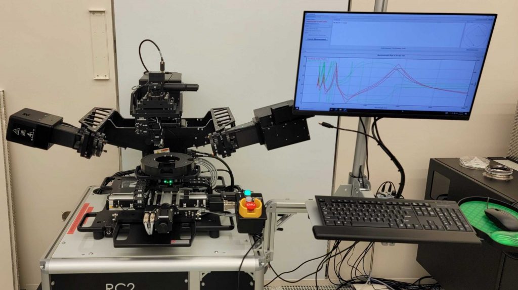
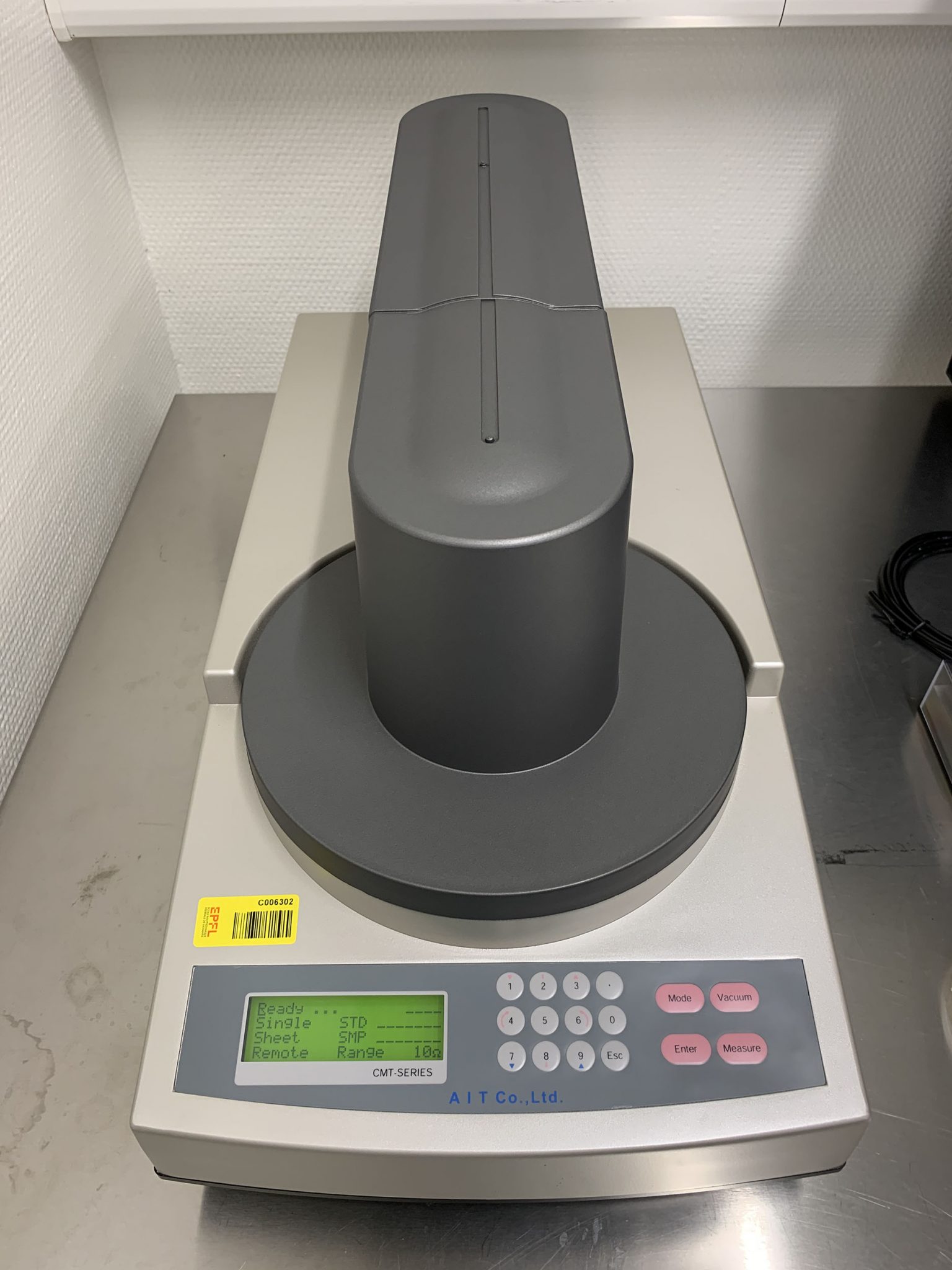
Electrical measurement

- Equipement
- – AC and DC impedance measurements with up to 4 probes
– Tungsten tips with 12 and 7 µm radius
– Stage travel with fine and coarse mode, up to 150mm x 150mm
– Instruments: Agilent 4155B SPA (DC), Zürich Instruments MFIA (AC)
– Location: Zone 11 - Documentation
- – Equipment Description
– MPI TS150 User Manual - Responsibles
- J. Dorsaz
N. Piacentini
M. Pillon
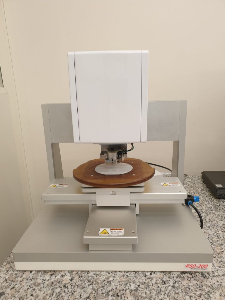
- Equipement
- – Compatible layers : Metal, Conductive Oxide, Silicon and Polysilicon.
The tool is configured by default for the metallic layers and for sample thickness of 525 um +/- 25 um.
If you are not in this configuration, please contact CMi staff
– Measurement range : 5 mOhm/sq to 5MOhm/sq
– Measurement area : 10x 10 to 200 x 200 mm
– Accuracy : +/- 1%
– Repeatability : < 0.5 %
– Temperature compensation
– 2D and 3D mapping
– Location: Zone 4
- Documentation
- – Manual
- Responsibles
- D. Bouvet
A. Toros
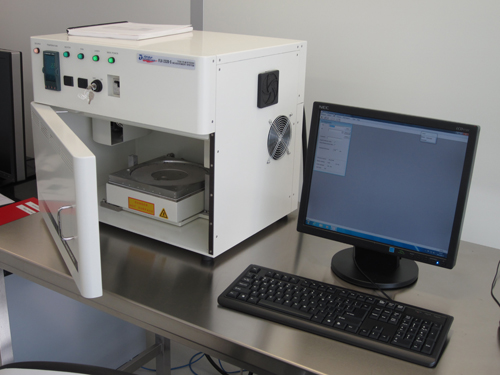
- Equipement
- – Compatible layers : Metal, Conductive Oxide, Silicon and Polysilicon.
The tool is configured by default for the metallic layers and for sample thickness of 525 um +/- 25 um.
If you are not in this configuration, please contact CMi staff
– Measurement range : 1 mOhm/sq to 2 MOhm/sq
– Measurement area : up to 8”/200 mm wafer, up to 6 mm thickness
– Accuracy : +/- 0.5%
– Temperature compensation
– 2D and 3D mapping
– Location: Zone 18
- Documentation
- – Specifications
– Manual - Responsibles
- D. Bouvet
A. Toros
Optical microscopy
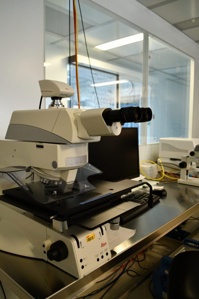
- Equipements
- – List of microscopes at CMi
- Documentation
- – Manual Leica D800