To be read first:
- Working with small chips: There is a risk of crashing the writehead on the sample, inducing major equipment downtime, if the standard operating procedure for loading is not followed accurately. Make sure to call the CMi staff if you are unsure how to proceed!
- Working with small chips: minimum chip size 5mm * 5mm.
- The equipment is sensitive to airborne solvent contamination on optical elements, and is equipped with charcoal filters. Always double-check that the window bay is closed when leaving the tool!
RESERVATION RULES AND BOOKING FEES POLICY:
- Booking: maximum 10 time slots allowed at any time.
- Users with long CAD conversion times (>1 hours) are encouraged to book overnight or during the weekends.
- Reservation names must correspond to operators.
- Billing : 6 minutes + processing time.
- This equipment is subject to penatly fees in case of user’s no-show.
Contents:
I. Introduction
The MLA150 is a Mask-Less Aligner developed by Heidelberg Instruments GmbH in Germany. This system allows researchers to quickly print a design, without the need to order or produce a mask, by exposing the photoresist with a UV laser (375 or 405 nm) focussed and scanned over the wafer.
The MLA can convert CAD-generated layout of standard file formats (.gds, .cif, .dxf), then align (top- and backside) and expose it on a substrate within a few minutes.
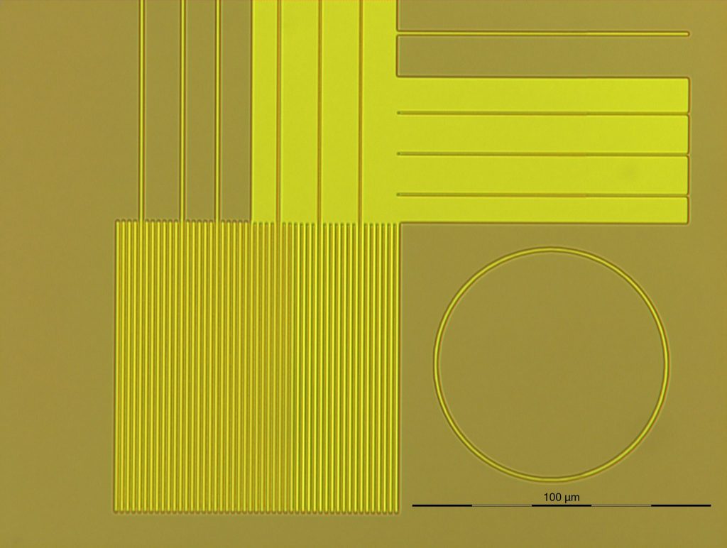
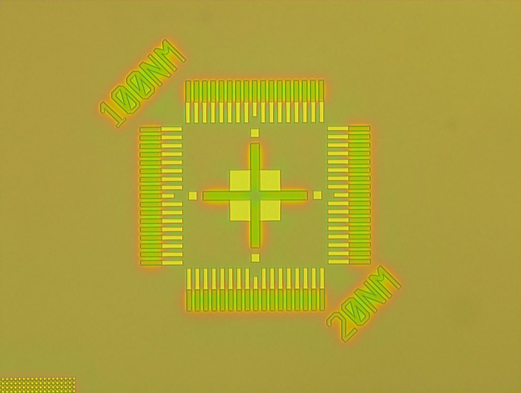
The resolution is limited by the photoresist, wavelength and resolving power of the optics (NA, depth of focus), and can reach a minimum of about 1 um with thin photoresist (PR) thickness (< 1 µm).
II. Equipment description
Equipment configuration:
The MLA150 system is equipped with:
- Exposure source: 405 nm or 375 nm laser diodes
- 3 cameras: overview for quick crosses localization, macro and micro for automatic detection of alignment crosses
- Optics for top-side and back-side alignment
- Real time autofocus
- Stage system, position control with interferometers, chuck with vacuum for various substrate sizes
Equipments specifications:
| MLA 150 | 1 | 2 |
|---|---|---|
| Maximum substrate size | 220 x 220 x 8 mm | 200 x 200 x 12 mm |
| Minimum substrate size | 5 x 5 x 0.1 mm | 5 x 5 x 0.1 mm |
| Minimum feature size | 1 um | 1 um |
| Uniformity | < 120 nm | < 120 nm |
| FSA accuracy | < 500 nm | < 500 nm |
| BSA accuracy | – | < 1000 nm |
| maximum exposure area | 150 x 150 mm | 150 x 150 mm |
| 405nm Laser power | 8000 mW | 8000 mW |
| 375nm Laser power | 2800 mW | 7200 mW |
| Writing time with 405nm laser (100 mm wafer) | < 9 min (Fast mode) | < 9 min (Fast mode) |
| Writing time with 375nm laser (100 mm wafer) | < 32 min (Fast mode) | < 9 min (Fast mode) |
| Top surface | Back surface | |
| High Res | 190x140um | – |
| Low Res | 640x480um | 640x480um |
| Overview | 12x9mm | – |
Overview camera cannot access the entire surface of the substrate due to mechanical limits
Size limitation and pneumatic autofocus:
Due to the pneumatic focus design, the surface of the sample must be such that a 5×5 mm square can be entirely contained within it as presented below.
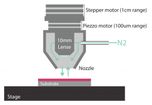
To probe the distance, compressed gas passes through the write head and leaves it through a nozzle. Once the write head is close enough to the substrate, a pressure builds up between the nozzle and the substrate, which is monitored by a pressure sensor. The pressure sensor transmits the signal to a controller which regulates the distance to the substrate through a piezzo.

The limit of 5x5mm is mandatory to ensure that the pressure builds up correctly when initially loading the substrate. Smaller, the risk of mismeasurement that will lead to a crash is too high !
If you have to expose a sample that does not respect the limitations, please contact the process engineer to find a solution. One would be to create a cavity the size of your sample in a carrier wafer, as presented in the image below.

Exposure parameters:
The MLA150 is an intuitive tool. Wafer position is automatically detected and the laser is directly focused at the center of the wafer after loading. Users should set only two parameters:
- Dose [mJ/cm2] : Keep in mind that the light source and exposure conditions are not the same as with a mask aligner so optimal dose and exposure results will be different.
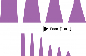
- Defocus [-] : Defines where the focus is done. A positive defocus will shift the focus downwards inside the resist (range: -10 .. +10, 10 being a shift of about 6 microns).
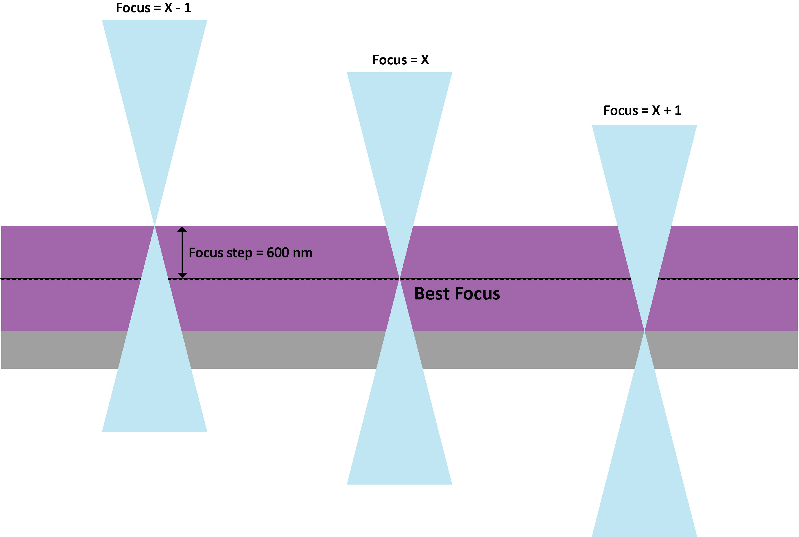
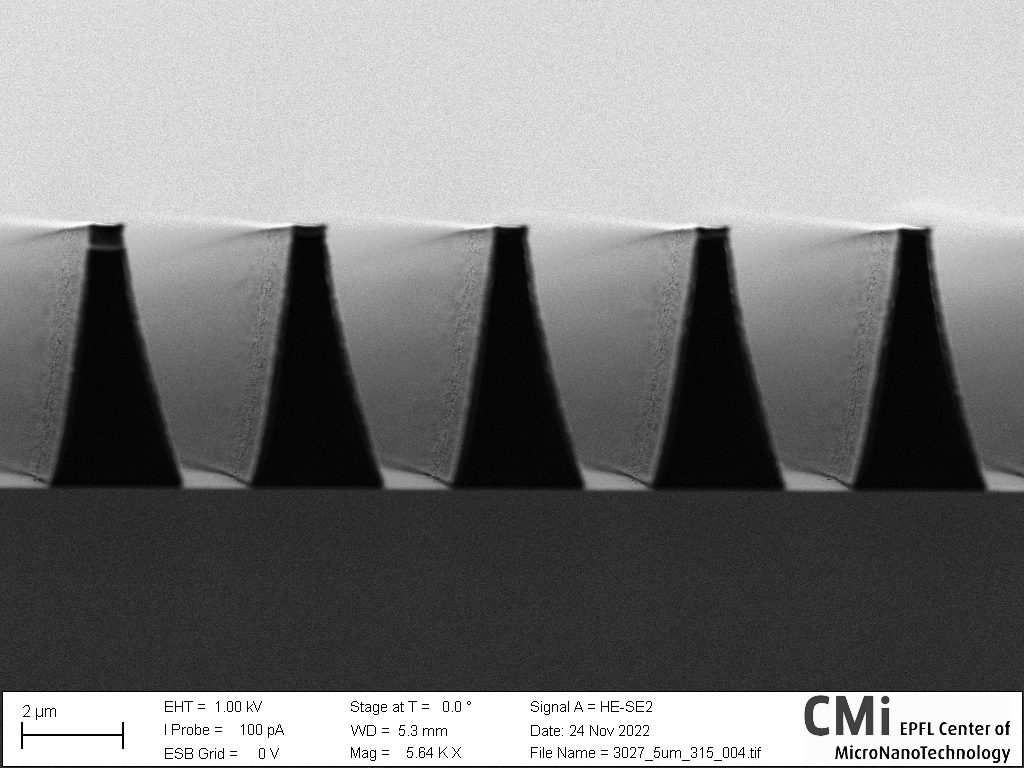
With positive photoresists, in practice both positive and negative defocus have the same effect. See below the impact on narrow and large isolated line.
Additionals features with MLA 150 – 2:
High aspect ratio (HAR)
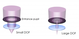
In this mode, the numerical aperture is reduced to improve depth of field. It can be considered when using a photoresist layer with thickness over 100um. Be aware that a higher dose is needed when using HAR. Two options are possible:
- Large : aperture diameter = 10%
- X-Large : aperture diameter = 5%
Greyscale :
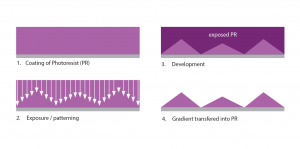
Grayscale lithography creates three-dimensional micro-structures with height gradients in a low-contrast positive phooresist (i.e series ma-P 1200G). The exposure depth is precisely controlled by modulating the laser intensity. The latter is converted into exposure depth and subsequently into resist topography on the micro-scale.
If you are interested in using the grayscale capabilities of the MLA150-2, you will find more information on this page.
