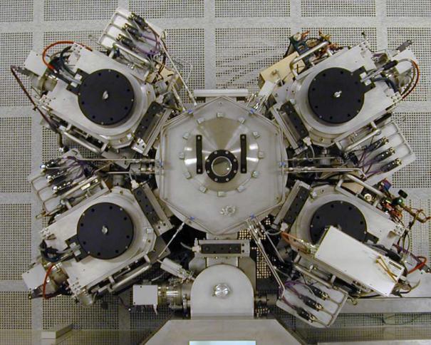
LPCVD / Dry or wet oxidation / Alloying / Doping / Diffusion / Densification / Annealing
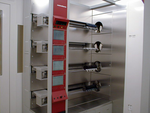
- Equipement
- – 6 x LPCVD tubes
– 1-1 polysilicon, amorphous silicon
– 1-2 stoichiometric silicon nitride Si3N4, low stress silicon nitride SixNy
– 3-1 low temperature oxide (LTO), undoped oxide, PSG, BPSG, BSG
– 3-2 TEOS
– 4-1 stoichiometric silicon nitride Si3N4, low stress silicon nitride SixNy
– 4-2 high temperature oxide (HTO), undoped oxide
– 5 x Oxidation tubes
– 2-1 dry oxide, densification
– 2-3 dry oxide, very clean processes for gate oxide
– 2-2 wet oxide
– 3-4 wet or dry oxide or annealing for non-microelectronic compatible processes
– 4-3 wet oxide
– 2 x Diffusion tubes
– 2-4 wet oxide, dopants diffusion, tube made of SiC for very high temperature processes (up to 1250°C)
– 4-4 annealing, tube made of SiC for very high temperature processes (up to 1250°C)
– 1 x Alloying tube
– 1-3 alloying of silicon and aluminum at junctions
– 1 x POCl3 doping tube
– 1-4 “N” doping (Phosphore) of silicon and polysilicon
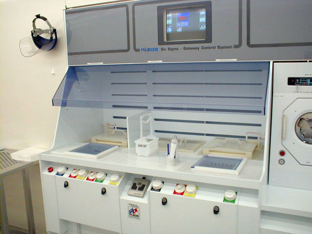
– RCA cleaning mandatory before oxidation & LPCVD
– Location: Zone 3 - Documentation
- – Manual
- Responsibles (Process)
- D. Bouvet
A. Toros
R. Juttin - Responsibles (Maintenance)
- N. Roch
M. Marmelo
P. Madliger
- Equipement
- – RCA cleaning mandatory before oxidation & LPCVD
– Non CMOS compatible materials are prohibited in this bench
– Location: Zone 3 - Documentation
- – Manual
- Responsibles (Process)
- D. Bouvet
G. Kumuntu - Responsibles (Maintenance)
- P. Madliger
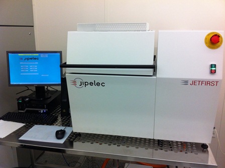
- Equipement
- – For activation and crystallization processes
– Flash head : 6 lamps (3 lamp circuits, 2 lamps each)
– Power supply : 160 W each circuit
– Vacuum system with inert gas supply and IR heater (up to 880°C)
– Substrate size : 4 inch wafer (thickness max. 2mm)
– Pulse duration : 0.35 to 13.9 ms
– Max energy : 4 to 55 J/cm2
– Location: Zone 8 - Documentation
- – Manual
- Responsibles (Process)
- A. Toros
- Responsibles (Maintenance)
- N. Roch
ALD
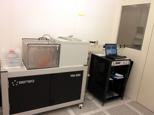
- Equipement
- – MANDATORY : A dummy Si chip (available next to the tool) has to be loaded in the chamber during each deposition !
– Thermal deposition
– Plasma assisted deposition
– Ozone generator
– Deposition temperature from 80°C to 300°C
– Available materials : Al2O3, TiO2, HfO2, SiO2, Pt
– Location: Zone 4 - Documentation
- – Manual
- Responsibles (Process)
- D. Bouvet
A. Toros - Responsibles (Maintenance)
- N. Roch
M. Marmelo
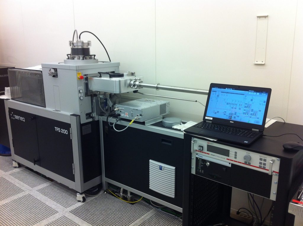
- Equipement
- – MANDATORY : A dummy Si chip (available next to the tool) has to be loaded in the chamber for each deposition !
– Thermal deposition
– Plasma assisted deposition
– Ozone generator
– Deposition temperature from 100°C to 300°C
– Available materials : Al2O3, TiO2, SiO2, AlN, ZnO, Ni, NiOx
– Location: Zone 4 - Documentation
- – Manual
- Responsibles (Process)
- D. Bouvet
A. Toros - Responsibles (Maintenance)
- N. Roch
M. Marmelo
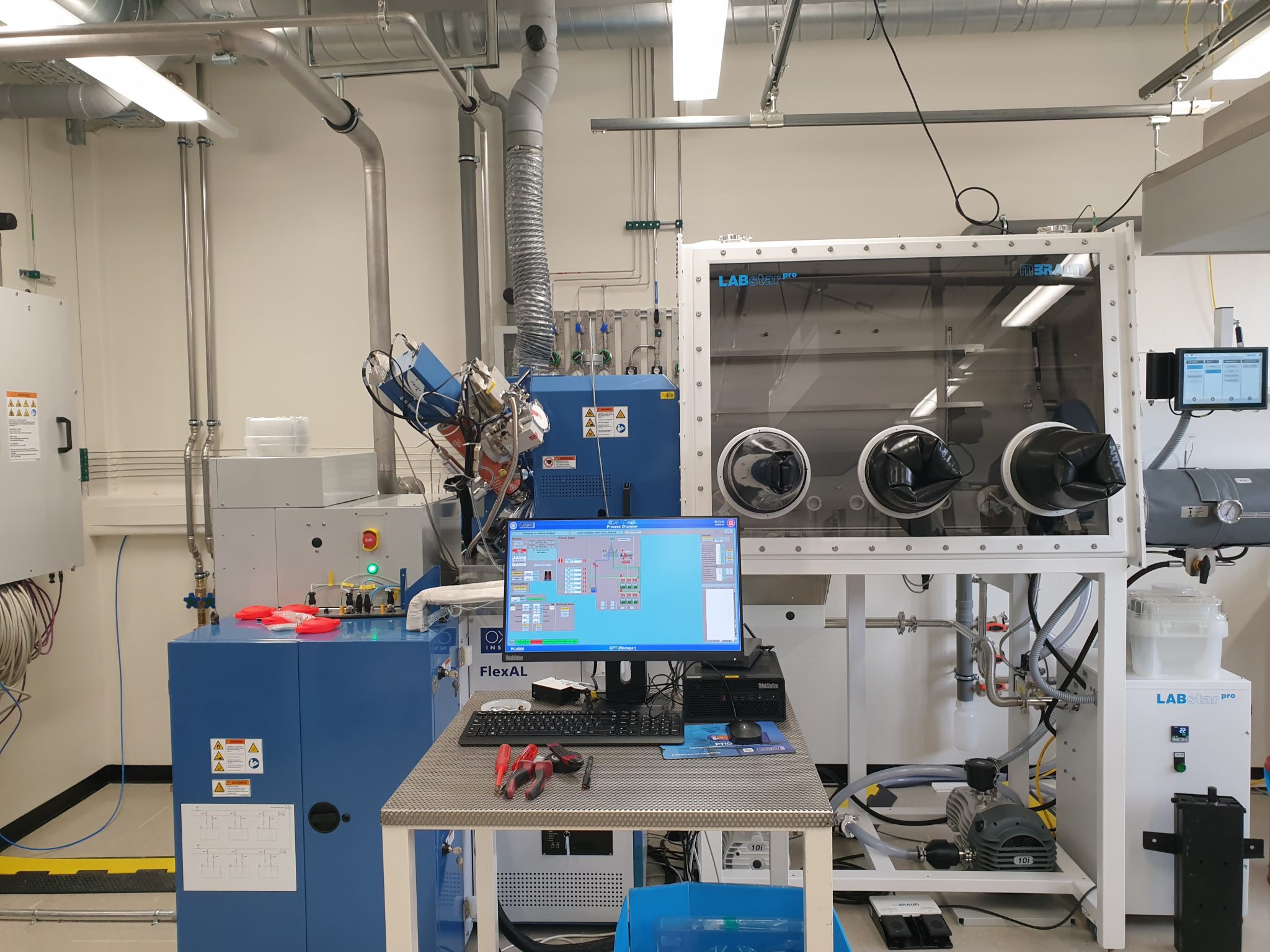
- Equipement
- – Sample holder for wafers up to 200mm
– Remote plasma and thermal ALD
– Ozone generator
– Deposition of high-quality nitride superconductors (NbN, TiN)
– Combined inert gas atmosphere glove box for sample preparation and loading
– Residual gas analyser
– Integrated optical emission spectrometer
– Heated chamber up to 150°C
– Heated substrate holder up to 550°C
– Location: Zone 18 - Documentation
- – Manual
- Responsibles (Process)
- D. Bouvet
A. Toros - Responsibles (Maintenance)
- N. Roch
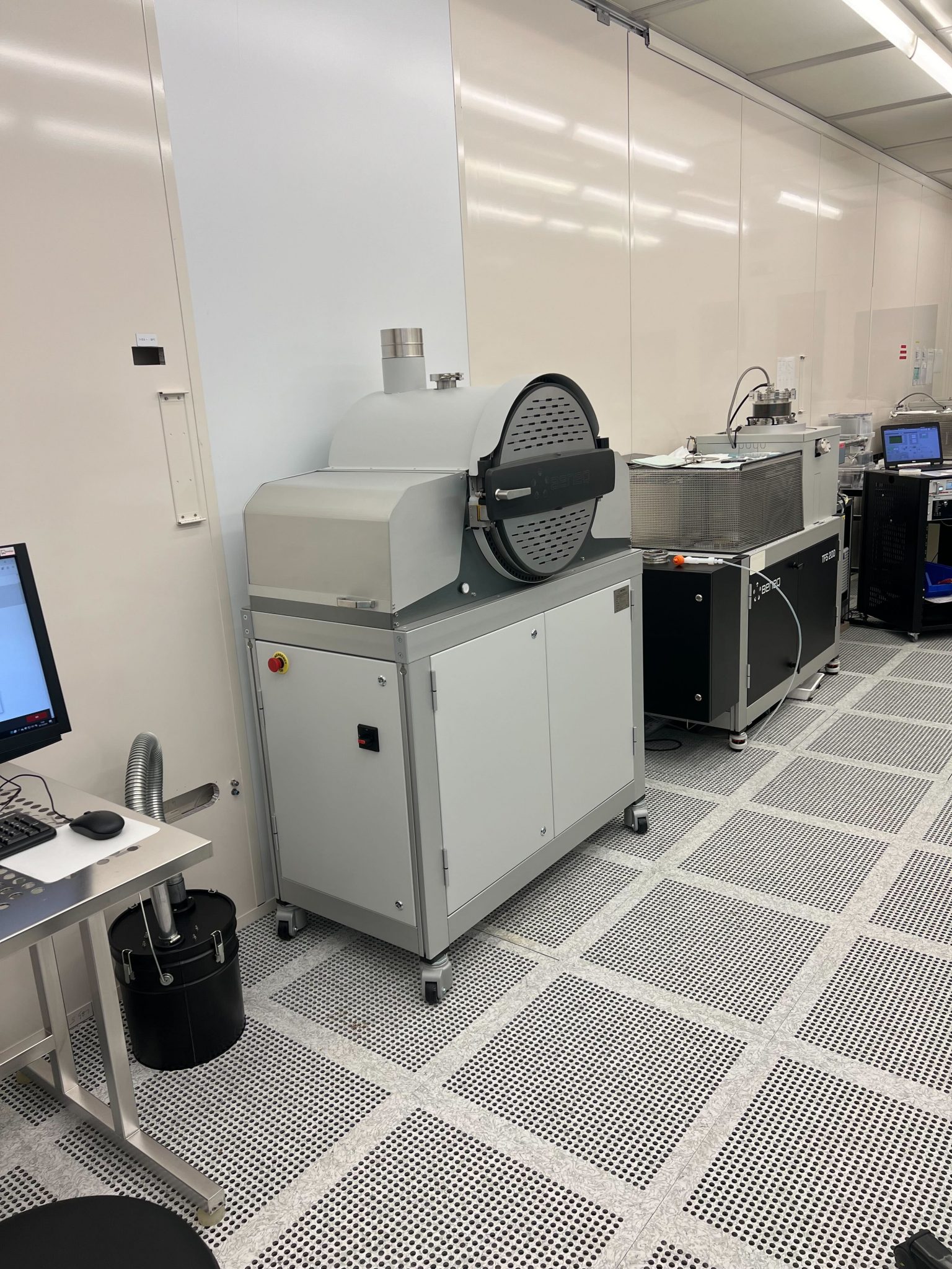
- Equipement
- – MANDATORY : A dummy Si chip (available next to the tool) has to be loaded in the chamber for each deposition !
– Thermal deposition
– Ozone generator
– Deposition temperature from 90°C to 250°C
– Available materials : Al2O3, HfO2
– Location: Zone 4 - Documentation
- – Manual
- Responsibles (Process)
- D. Bouvet
A. Toros - Responsibles (Maintenance)
- N. Roch
M. Marmelo
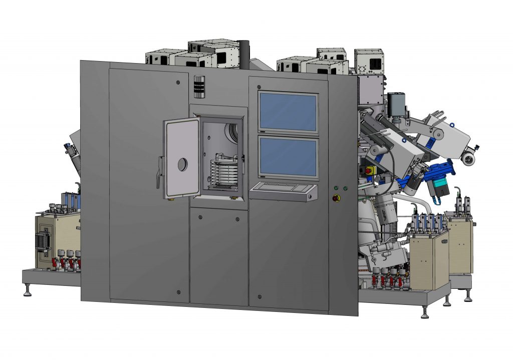
PECVD
The ICP CVD is for the moment only accessible to LPQM lab members for development.
- Equipement
- – PlasmaPro 100 platform equiped with an Inductively Couple Plasma Chemical Vapor Deposition (ICP CVD) process module.
– 5kW ICP Plasma deposition source
– RF 600 W generator for etch
– Up to 400°C table temperature
– From 100mm to 200mm wafers
– Location: Zone 3 - Documentation
- Manual
- Responsibles
- B. Cuénod
R. Juttin
O. Feijo
Evaporation
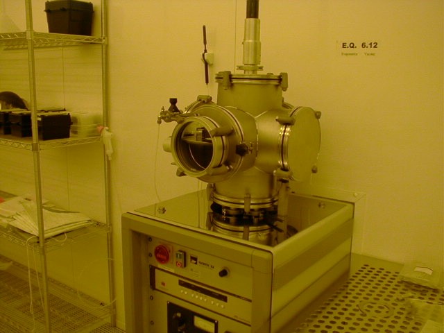
- Equipement
- – Dedicated to the coating of thin conductive layers to prevent charging issues during e-beam exposure (Cr).
– 4 x boats for thermal evaporation.
– Loadlock to speed up the substrate loading/unloading (1 x 100 mm wafer at a time).
– Location: Zone 11 - Documentation
- – Manual
- Responsibles
- R. Juttin
B. Cuénod
T. Tarasi
- Equipement
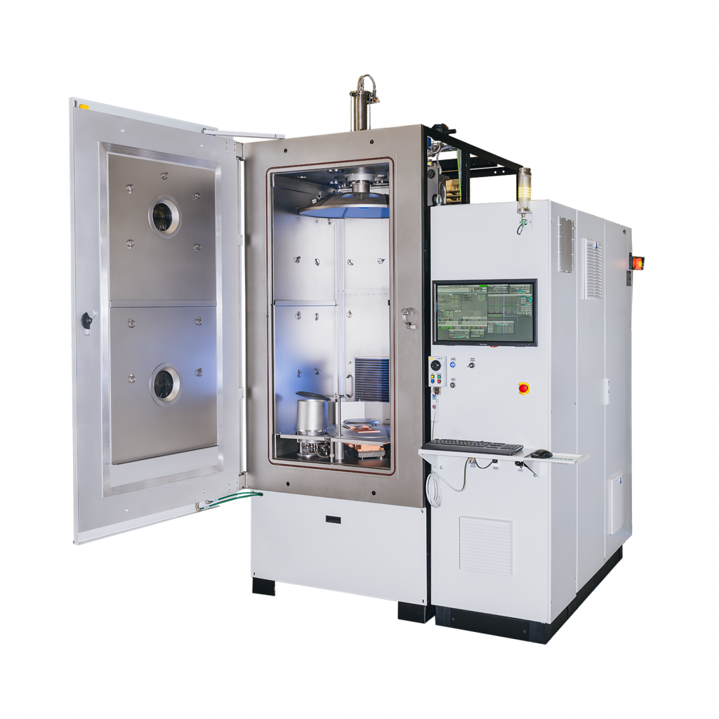
- – 1 x e-beam gun (6 pockets)
– 1 x ion source (Ar, O2) for Ion Assisted Deposition (IAD)
– Chamber designed for lift-off evaporation (high distance source-substrates)
– Heaters (evaporation from room temperature and up to 200°C)
– Up to 8 x 100 mm or 4 x 150 mm wafers
– Location: Zone 4 - Documentation
- – Manual
- Responsibles
- R. Juttin
G. Clerc
B. Cuénod
T. Tarasi
The new evaporator is now available to users. Please note that not all materials are available yet. Contact the tool responsibles below for more information.
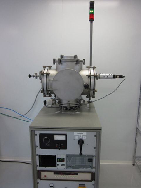
- Equipement
- – 2 x boat for thermal evaporation
– Location: BM 4231 - Documentation
- – Manual
- Responsibles
- The system is now under the responsibility of BIOS laboratory.
Contact: Felix Richter
- Equipement
- – 3 x boat for thermal evaporation
– Location: MC A3 205 - Documentation
- – Manual
- Responsibles
- The system is now under the responsibility of AQUA laboratory.
Contact: Ekin Kizilkan
Sputtering
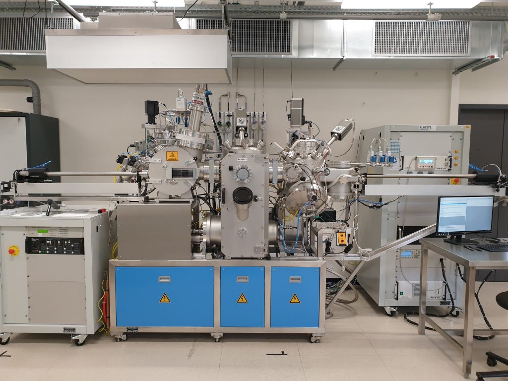
- Equipement
- 5 x modules [+ Load lock & Transfer module]:
– N°2 – Oxides & Nitrides (3 x cathodes Ø 100 mm confocal,
RF/DC-pulsed)
– N°3 – UHV Ferromagnetic metals & Metals (4 x cathodes Ø 100mm confocal, RF/DC-pulsed + HIPIMS)
RF/DC-pulsed)
– N°4 – Dielectrics (1 x cathode Ø 250mm, planar,
RF-Sputtering)
– N°5 – UHV Semiconductors & Metals (4 x cathodes Ø 100mm confocal, RF/DC-pulsed + HIPIMS)
– N°6 – Nitrides (3 x cathodes Ø 100 mm confocal,
RF/DC-pulsed)
Process:
– Deposition at Room Temperature or High Temperature
– RF-Etch for substrate cleaning or activation prior deposition
– Up to 200 mm wafers
– Location: Zone 4 - Documentation
- – Manual
- Responsibles
- R. Juttin
B. Cuénod
G. Clerc
T. Tarasi
Pulsed Laser Deposition
Electroplating / Parylene coating
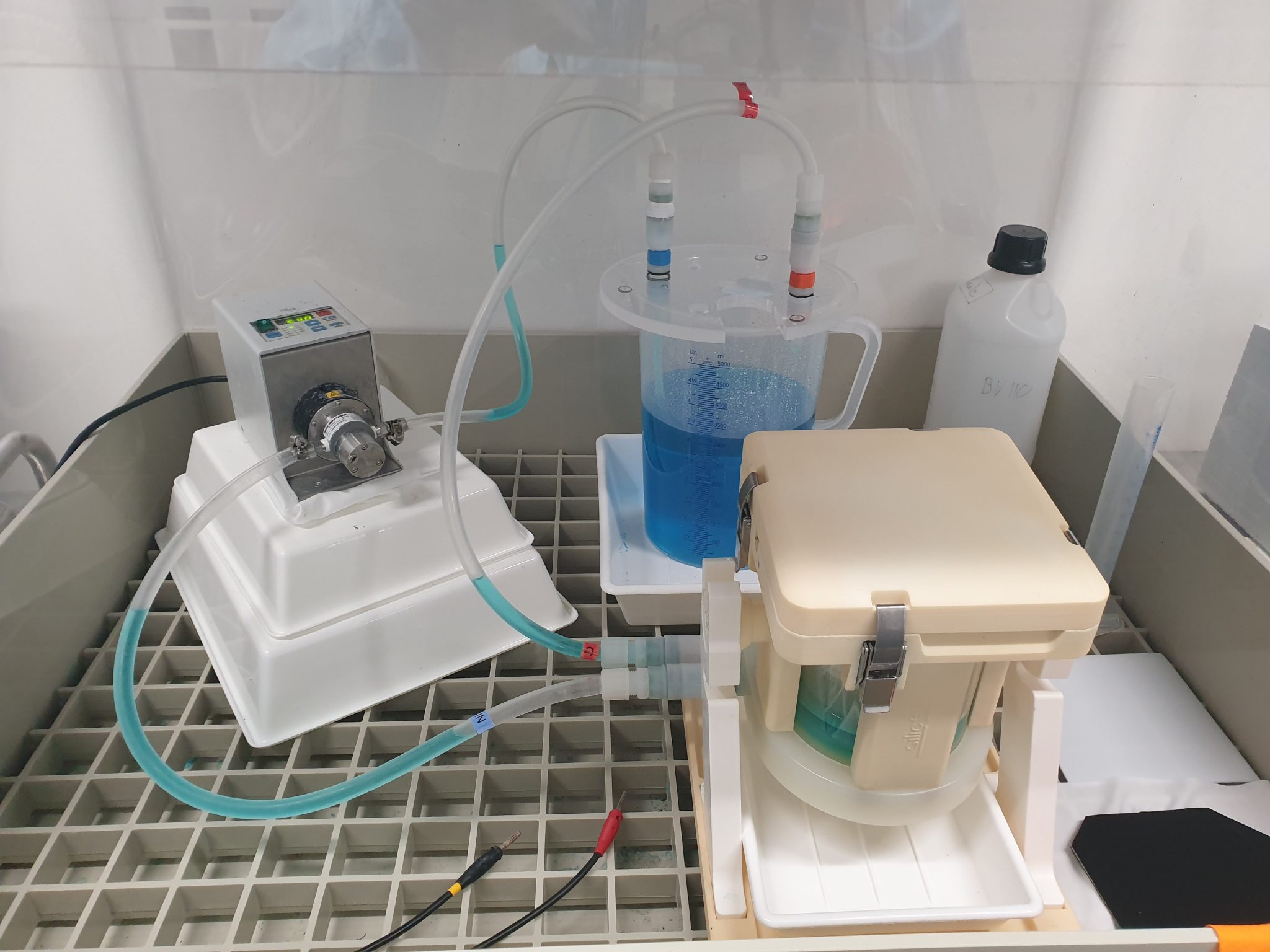
- Equipement
- – Copper electroplating
– Compatible with 100 mm wafers only
– Deposition rate : ~100-200 nm/min
– Location: Zone 19 - Documentation
- – Manual
– Plating solution datasheet - Responsibles
- D. Bouvet
A. Toros
- Equipement
- – Any kind of wafers and samples coating
– Parylene C
– Biocompatible material
– Thickness range from 50nm up to 10um
– Room temperature and double side coating
– Conformal and stress free layer
– Acids, bases and solvents resistant layers
– Location: Zone 10 - Documentation
- – Manual
– Silanization
– Recristallization - Responsibles
- C. Hibert
M. Marmelo
MPCVD
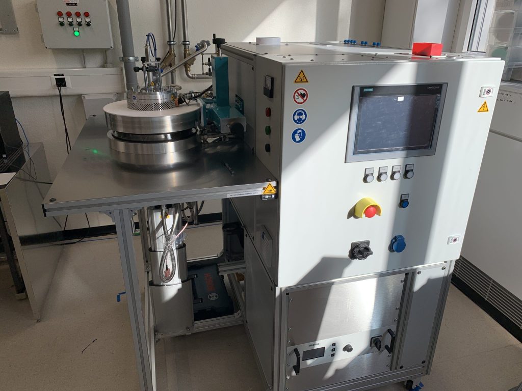
- Equipement
- – 6” plasma CVD system (2.45 GHz)
– CVD diamond synthesis/coating
– Diamond, silicon and molybdenum as substrate materials
– Process gases : H2, CH4, Ar, CO2, N2
– 2 exchangeable substrate holders : one equipped with cooling element for single crystal CVD growth at high growth rate, one with a heating element for polycristalline diamond film growth in electronic grade
– Heated holder diameter 100 mm
– Cooled holder diameter 60 mm
– Optical emission spectroscopy
– Camera for visual control of process
– Location: Zone 19 - Documentation
- – Manual
- Responsibles
- A. Toros