No training on this tool, only batch service on request organized every Thursday
Please see chapter 3: steps to request and participate to a parylene run
Equipement main features:
- Any kind of wafers and samples coating
- Parylene C
- Biocompatible material
- Thickness range from 50nm up to 10um
- Room temperature and double side coating
- Conformal and stress free layer
- Acids, bases and solvents resistant layers
- Location: Zone 10
I. Introduction
Parylene can be use as a:
- Protective or support layer for sensitive device
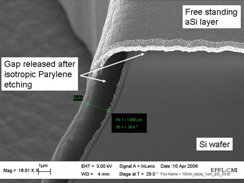
- Sacrificial layer with Al or Si device
- Device layer with PR, SiO2 or Si as a sacrificial layer
II. Principle of deposition
Parylene raw material is a solid dimmer. The system works under a primary vacuum (few µbar). The dimmer is heated at about 150°C and changes to a vapor phase. It diffuses to Pyrolysis chamber at 670°C and is dissociated in a monomer. The monomer diffuses to the room temperature or slightly heated (80°C) process chamber, and condensates to fabricate Parylene layer. Before being pump, residual monomers are trapped in a cryogenic device.
The layer thickness depends on the Parylene solid load placed in the vaporization boat. Total surface and arrangement in the processing chamber influence the thickness and uniformity. At 100 mm Silicon wafer scale layer uniformity is less than 1%.
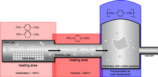
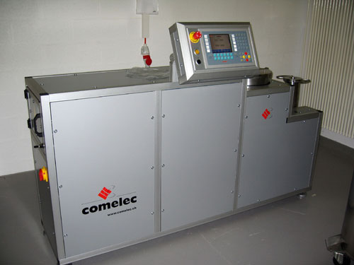
figure 1: Parylene coating tool (Courtesy of www.comelec.ch)
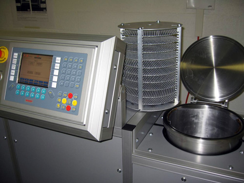
figure 2: Parylene front panel, 10 slots holder and processing chamber
Parylene Load Estimation for CMi C-30-S tool
| Parylene load (g) | 0.2 | 7.0 | 11.0 |
|---|---|---|---|
| Avg. thickness | 62 nm | 2.09 µm | 3.15 µm |
III. Steps to request and participate to a parylene run
- If you are a CMi users: make a parylene request deposition using this link request
- If you are not a CMi user contact infocmi@epfl.ch
- Fill the parylene form: PARYLENE SERVICE REQUEST FORM E Mail (EDIT) V3
- If relevant, protect one side of your sample(s) or your wafers(s) with:
- UV tape (chips and wafers),
- A dummy wafer fixed with to pieces of kapton tape,
- Tape for chips.
- If relevant, get your material outside of the cleanroom,
- In the clean room, place your material in a clean box (white box for wafers)
- place the box in a plastic bag available in the -1 material sas in CMi
- transfer the materail outside of the cleanroom.
- Place your material and the parylene form in the parylene cabinet near the CMi secretary on the shelf parylene service IN, see figure 3.
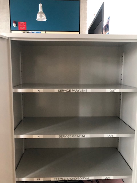
figure 3: service cabinet near CMi secretary BM1 124
- Once the run is finished you will get an email to invite you to collect your material in the service cabinet OUT shelf.
IV. Photos gallery
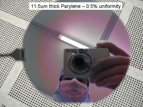
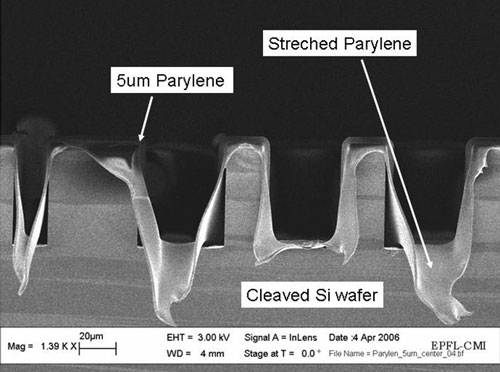
Parylene conformal coating in deep Si cavities. Parylene is delaminated after sample cleavage. We can notice parylene is also ductile.
