Back to the current year Winners
2017, December
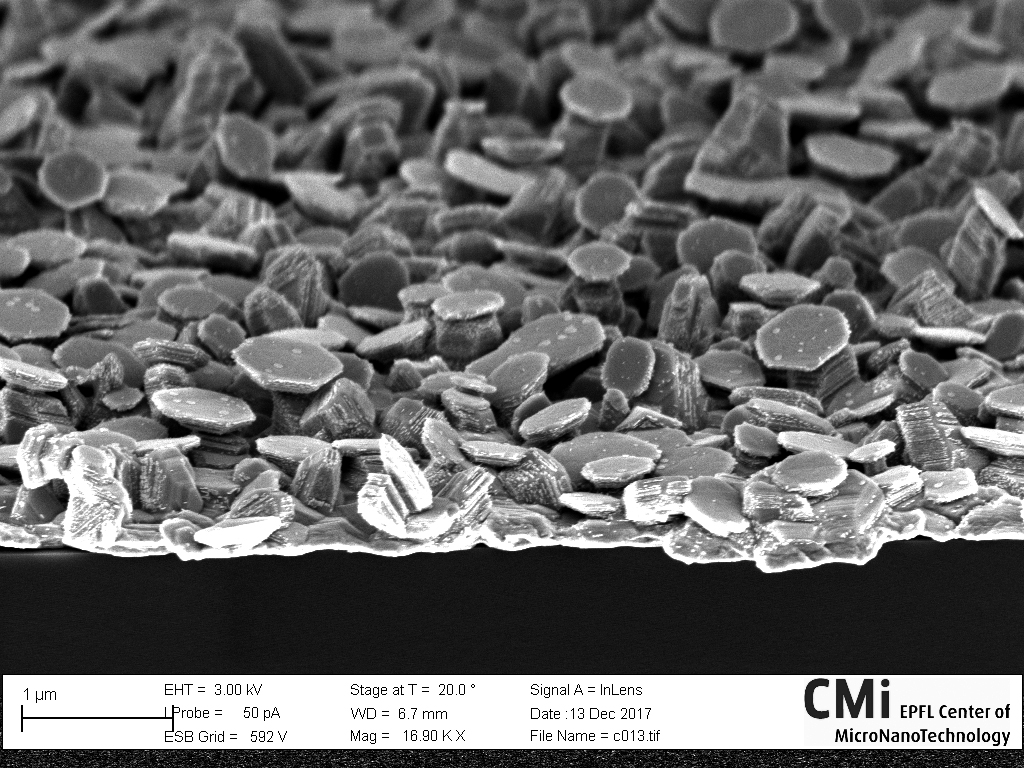
Zinc by MBE
Mahdi Zamani, LMSC
The attempt at growing zinc by Molecular Beam Epitaxy machine at 70 C results in the bacteria-like features depicted here. The low growth temperature prevents the merging of the platelets.

First snowdrops
Anastasiia Glushkova, LPMC
Morphology of methylammonium lead iodide. Surprisingly enough, some crystals just can’t help but being a flower.
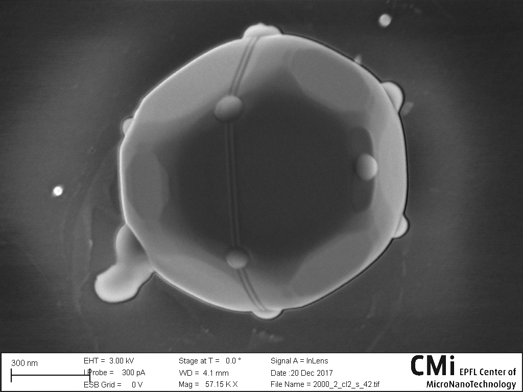
Gold planet with orbiting moon
Gaetan Bernard, LMSC
Gold nanoparticle prepared by dynamic templating has gold droplets on high energy regions and a double belt.
2017, November
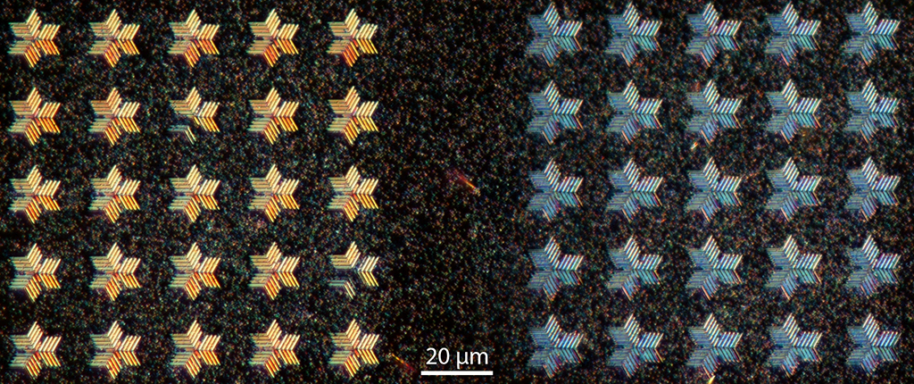
Fire and Ice
Martin Friedl, LMSC
It’s amazing what you can see with a simple optical microscope. Seen here are patterns of 70/100 nm wide and 300/600 nm tall GaAs fins standing vertically on a GaAs substrate. Normally you would have a hard time seeing them in an optical microscope, but we can play a neat trick! By tuning the microscope light polarization we can enhance their contrast and even resolve individual fins! The icing on the cake is that their orange and blue colour is a direct consequence of their geometry (height and width) which reflects only certain wavelengths of light! Nikon Optiphot 200 (Zone 15) – two stitched images.
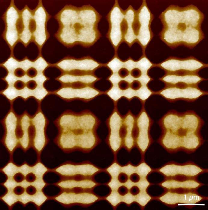
Phase shift kaleidoscope
Leo Garin, Kim Wonjong, LMSC
It is an AFM job done of a phase shift photo lithography. Everything has been done in CMi. From the mask, mask alignment crosses, phase shift photolithography and AFM job. The intent goal was to make an array of holes but two parameters seem off. First the space is not regular, it means that the mask is not the good length or not perpendicular enough. Second, there is only one out of two lines that is good, it can be that the steps are tilted regarding the incident light. But it still gives very homogeneous results over the whole sample, making this nice kaleidoscope-like pattern.
One snowy night
Kim Wonjong, LMSC
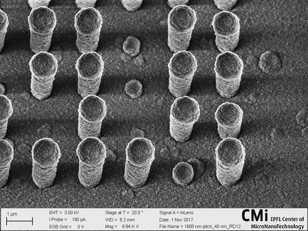
Here is the SEM image of one snowy night on nanowires world. Already we are close to the end of this year. I guess I am not the only one who wishes for snow. We could not bring the snow into the SEM so we decided to deposit PECVD grown oxide on our GaAs NW arrays. Image was taken in CMI, Zone 15, SEM Merlin.
2017, October
Carved in gold
Aqeel Ahmed, LQNO
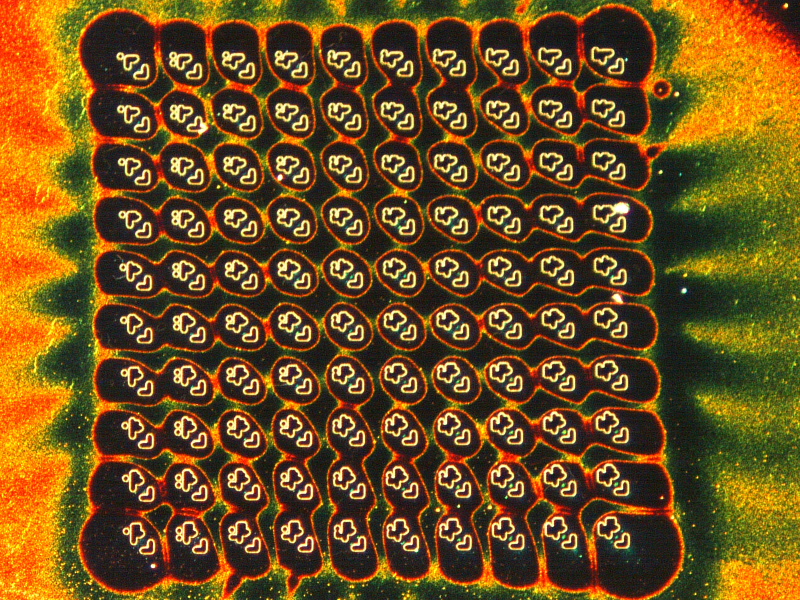
Markers on gold thin film produced by photolithography are viewed in dark-field microscope at 10X magnification. The image was taken right after Ion beam etching and before removal of photoresist. The distance between markers is 25um.
Wafer Firmament
Matthias Neuenschwander, LBNI
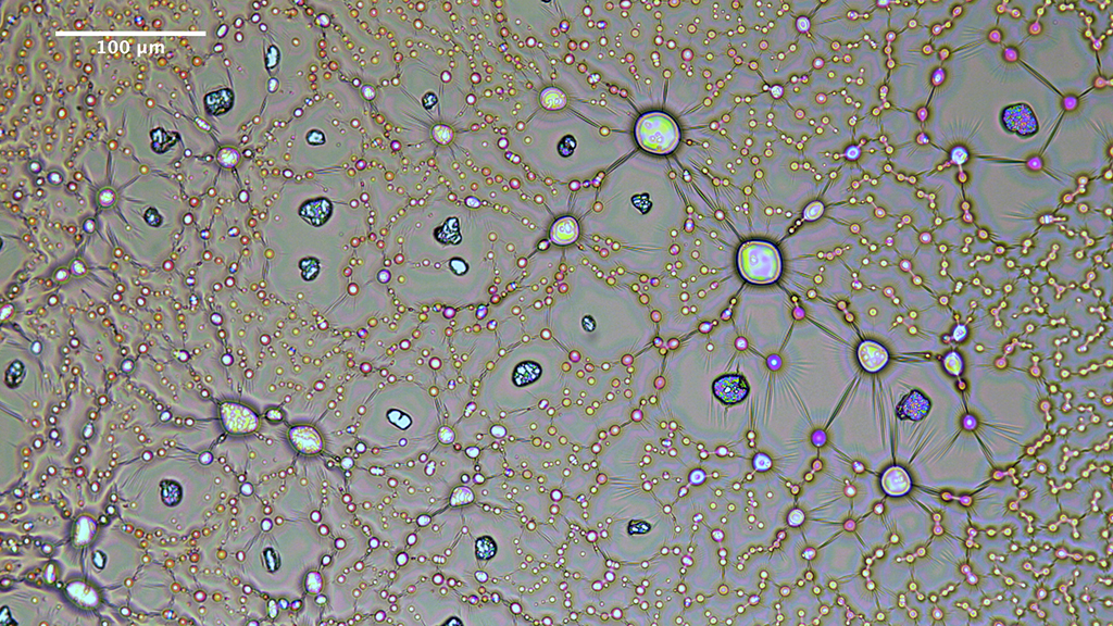
I (not-entirely on purpose) over-heated my photoresist. Now it is showing beautiful stellar constellations, some sort of star-spangled firmament covering a flat disc. Optical microscope image.
Golden anomaly
Aqeel Ahmed, LQNO
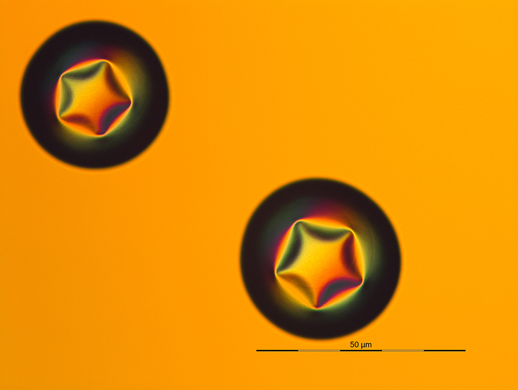
Anomalies formed on the surface on 100nm of Au evaporated on Si wafer. The image was taken at 20X magnification in bright-field microscope.
Giving life
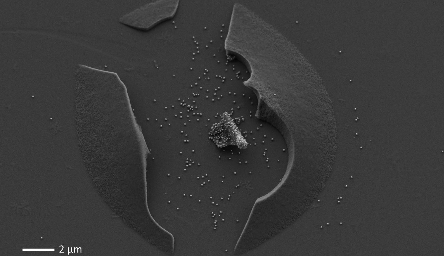
Lucas Guniat, LMSC
“Who would have thought that carrying a baby would be so hard, yet would give you so much love? Indeed, when this defect of an SiO2 oxide on top of a silicon wafer knew that it was expecting a surprise from our MBE (molecular beam epitaxy) machine, its first reaction was: “Oh sheesh, how long will this last? An entire growth time?”. But then, after several degassing steps and baking temperatures, the only question in its mind was: “Is it a Gallium droplet, or a GaAs compound?”. After the echography, we had the chance to put our hands on one of the photos. Of course, we didn’t reveal to the mom the true nature of its creation…”
Microfabrication to the extreme
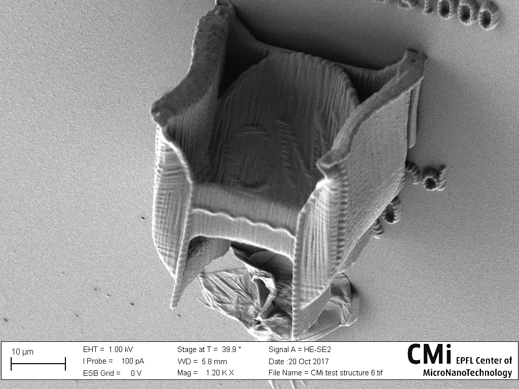
Julien Dorsaz, CMI
When scientists take miniaturization backwards! Instead of manufacturing the world smallest chips on a huge wafer, they decide to build a single-chip on the world smallest wafer. Here you can see a wafer inside its cassette printed in 3D, using two-photon absorption, with a Nanoscribe Photonic GT system. The wafer is about 20um in diameter. The whole structure collapsed during the development step due to insufficient polymerization of the Ormocomp negative resist.
2017, September
The Balance Of Nature
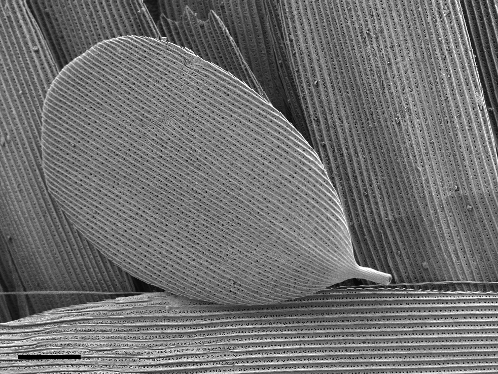
Marta Airaghi Leccardi, LNE
Benoit Desbiolles , LMIS4
Nano-fabrication technologies allows us to produce bio-inspired patterns responsible for specific physical phenomena. Here, we propose you a SEM image of the ideal pattern developed by Nature in order to generate colors of butterfly wings. Beautiful to the naked eye and even more at the micro-scale. Scale bar: 10um
Glass µ-cylinders
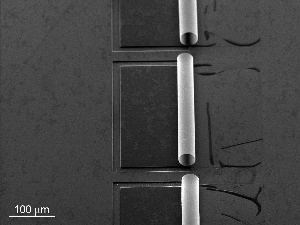
Esteban Bermudez Ureña, Soft Matter Physics, AMI
New stock of glass cylinders for your chemistry experiments. The image shows rolled-up SiO2 microtubes obtained after removing a sacrificial layer beneath a stressed SiO2 film. Substrate patterning, thin film deposition and etching was carried out at CMi. The roll-up process and tilted SEM imaging was performed at the Adolphe Merkle Institute in Fribourg.
2017, August
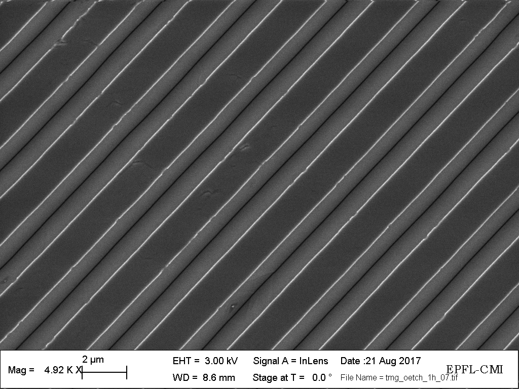
Groovy Diamond
Marcell Kiss, Q-LAB
Atomically smooth V-groove gratings are something we have all seen… the catch? These are fabricated in single crystal diamond instead of silicon, using an oxygen plasma etch instead of KOH/TMAH.

The Ring
Filip Boskovic, LBEN
The Ring is a traditional symbol of infinity or eternity, the transposition of the magic circle into the real world of tangible, functional objects. In a magical sense, wearing a ring binds you with power, with energy. The material (glass) of which the ring is constructed, plus your visualization (SEM), determine the nature of this energy (science). The appearance or attractiveness of a ring, or its material value, is of little importance in magic as well as in process of pushing capillaries to the nanoscale. Shrinking glass rings is all about magic – the transposition of the magic circle into the real world of tangible, functional glass nanocapillaries, commitment to the last breath.
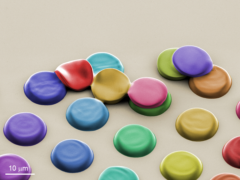
Confetti Minifab
Marta Airaghi Leccardi, LNE
Benoit Desbiolles , LMIS4
In view of a birthday party, we attempted to produce mini-confetti. The process involved a direct patterning of a photo-sensitive polymer, which is soft to the touch for the complete comfort of the customer. However, something went wrong… It seems that the color sorting tool could not follow the high manufacturing rate usually achieved at CMi. The quality control could record the consequences of this malfunctioning and send us an alert.
2017, July
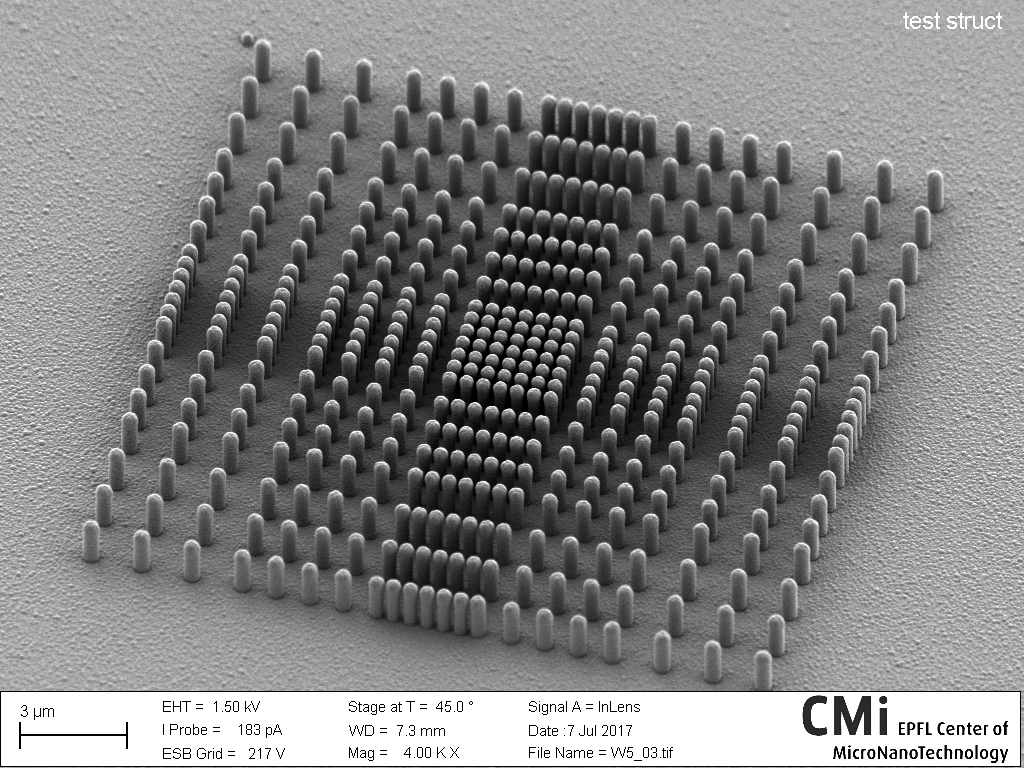
SiTONEHENGE
Stefano Varricchio, LMIS4
Ruins of prehistoric silicon nanopillars covered through the ages by a layer of SiO2. The utility of the structure is still uncertain, archeologist believe it delimits a burial ground for the hopes and dreams of PhD students working at night.
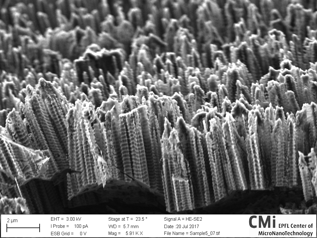
Hong Kong Skyscrapers
Ahmad Reza Motezakker, NEMS
This SEM image reminds me the Special Administrative Region of Hong Kong, the tallest urban agglomeration of the world. These beautiful structures are just silicon nano-grass which can be fabricated by Deep Reactive Ion Etching process. If you are looking for a super-hydrophobic structure, just grow them on the surface.
2017, June
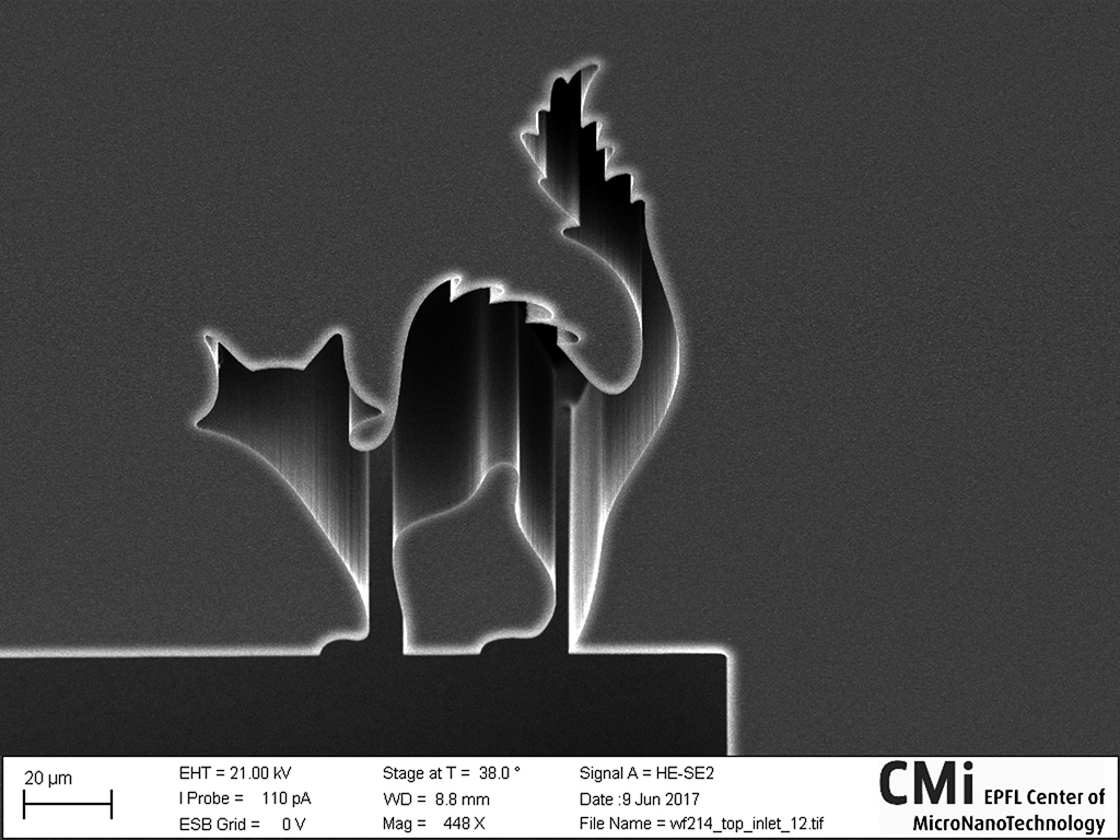
Silly cat contamination
Clementine Lipp, EP-DD-DT/CERN
Too much space on a silicon wafer for a standard DRIE and a silly designer might result in the apparition of wild silicate contamination.
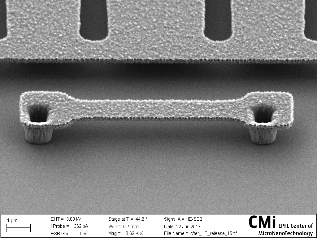
Freestanding micro-bridge
Adrien Toros, Q-LAB
This micro-bridge is one of the first structures released with the newly installed SPTS uEtch HF Vapor Etcher! The bridge and the pillars are made of Polysilicon, deposited on a patterned silicon oxide sacrificial layer. After patterning the Polysilicon layer, the silicon oxide was HF-vapor etched to release this 7 um long and 1um wide freestanding bridge. All fabrication steps were done at CMi with the VPG200 Laser writer, and three different etching tools : SPTS APS (Oxide etch), AMS200 (PolySi etch) and SPTS uEtch (HF Vapor release).
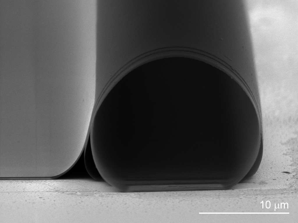
Swiss-roll
Esteban Bermudez, Soft Matter Physics, AMI
A new micro-tunnel for the Swiss tunnel network. The image shows what happens when a strained 50 nm thick layer of SiO2 is released from an underlying sacrificial layer: the film self-assembles into a Swiss-roll like structure. Substrate patterning and thin film deposition was carried out at CMi while the rolling and imaging was performed at the Adolphe Merkle Institute in Fribourg.
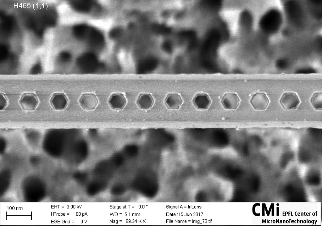
Nature’s Little Helper
Ian Rousseau, LASPE
Giovanni Santoruvo, POWERLAB
40 nm side length hexagonal holes with super sharp corners were made in a 300 nm thick gallium nitride membrane suspended over a silicon substrate by electron beam lithography, dry, vapor, and wet etching. The lithography and dry etching resulted in rounded corners, but, since the nanostructure was aligned with the epilayer crystal, anisotropic wet etching stopped on a pre-defined crystal plane. The hexagonal shape is caused by the of the wurtzite symmetry of the gallium nitride epilayer nano-bee-m.
Sitting Bull
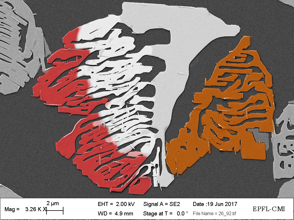
Michal Macha, LBEN
If you start seeing indian chiefs in your thin crystals, you know it is time to stop inhaling methanol in the lab. This very obvious picture, which was absolutely and undoubtedly what we wanted to achieve in this experiment, is a depiction of chief Sitting Bull. Made of Mo, S and O atoms. Although, if one rejects his imagination, one can say that the picture shows a Mo-oxysulfide crystals grown in chemical vapor deposition process on a Si/SiO2 wafer. This process is used to create mono-atomic layers of MoS2 which are used to e.g. fabricate single-molecule sensing devices. The structure seen on the picture, obviously not monoatomic, happens when you put “slightly” too much of the growth precursor inside CVD growth tube.
2017, May
Art of crystal 1
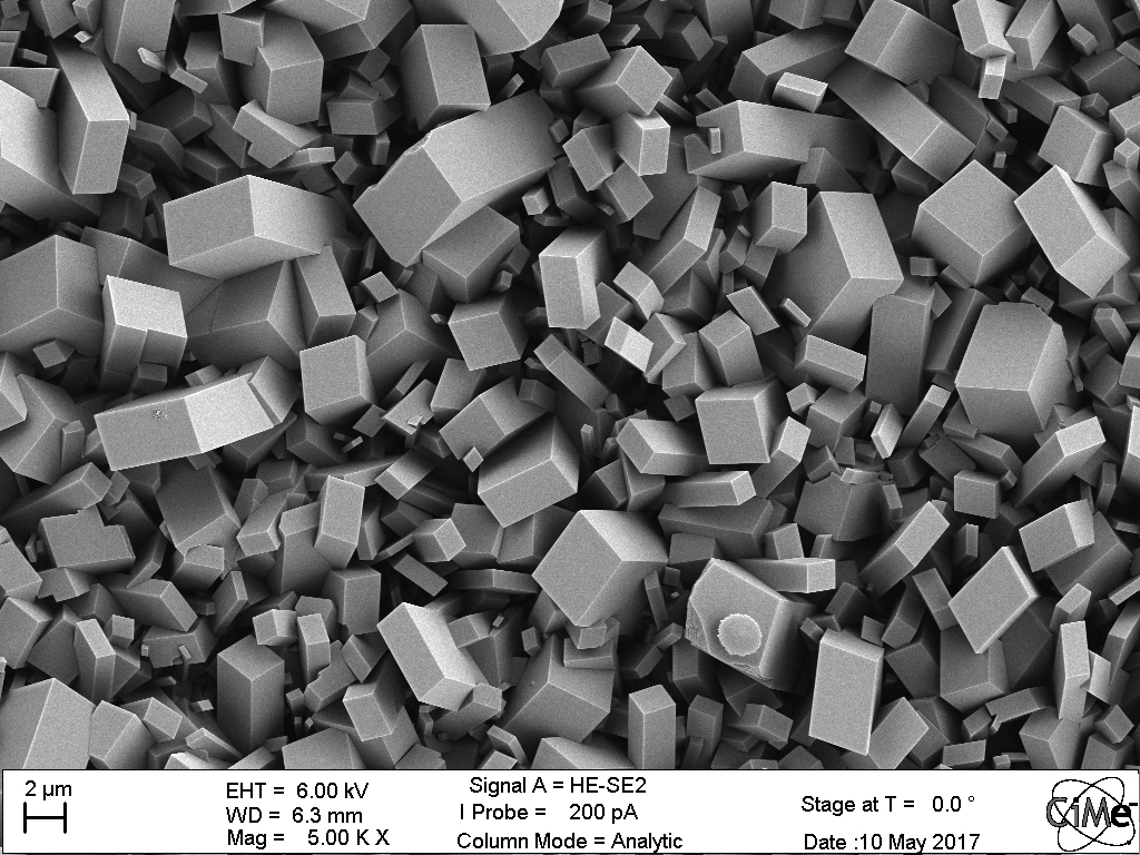
Huachuan Du, SMAL
This is a SEM image of calcium carbonate crystals produced by microfluidic spray dryer. The different morphology comes from their different crystalline structure. The spray dryer is fabricated by following the soft lithography protocol in CMi.
Art of crystal 2
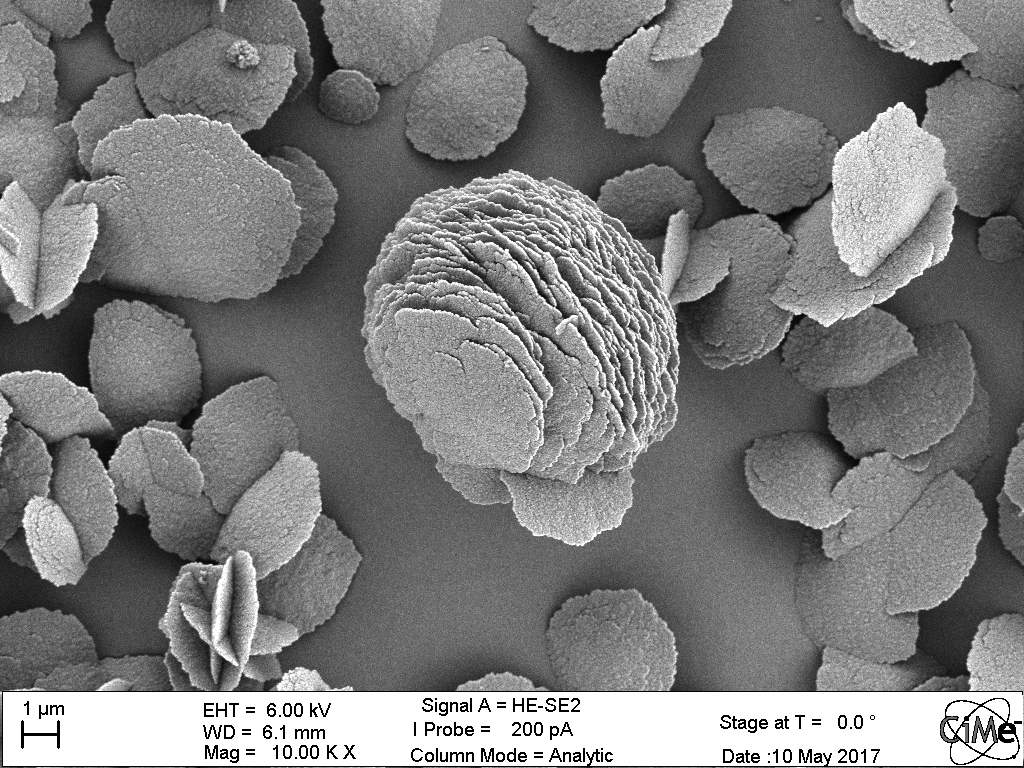
Huachuan Du, SMAL
This is a SEM image of calcium carbonate crystals produced by microfluidic spray dryer. The different morphology comes from their different crystalline structure. The spray dryer is fabricated by following the soft lithography protocol in CMi.
Crème caramel
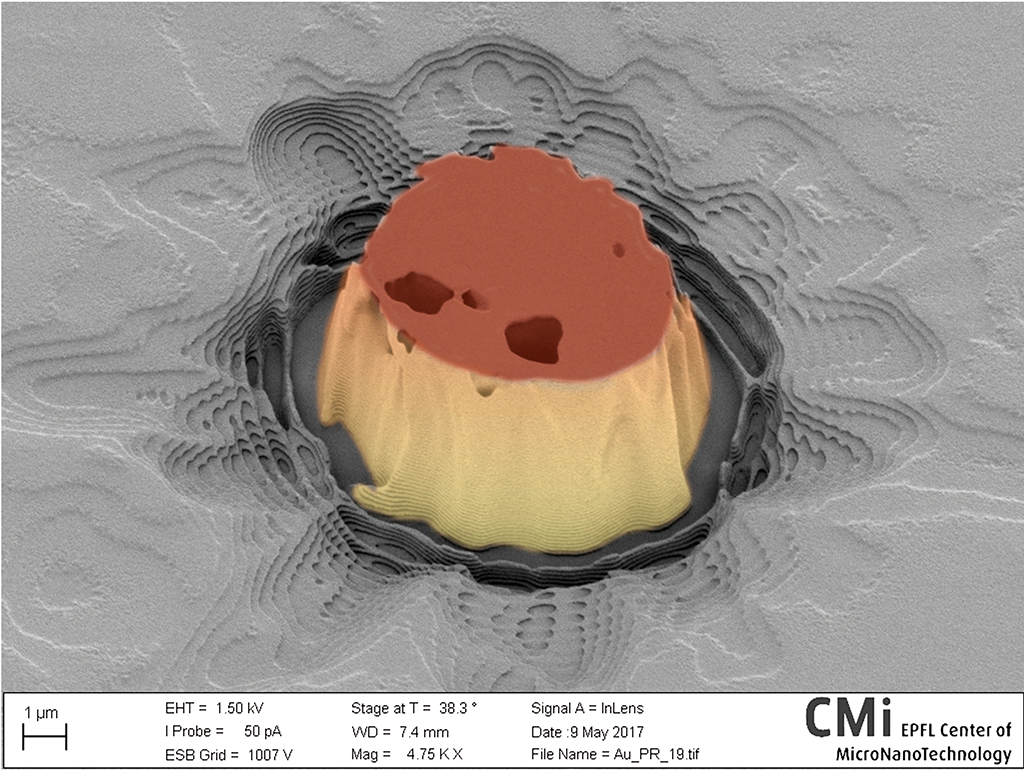
Hanie Kavand, Benoît Desbiolles, LMIS4
Say goodbye to nonsense recipes and try this fail-safe recipe. To cook the perfect crème caramel you will need: 80degC pre-baked PDMS, photoresist of choice, and some light to make everything bright. Mix well till everything comes together. And now for the final touch, garnish your dish with sprinkles of KOH. I prefer mine medium done and with just a little bit of garnish. Feel free to change the recipe according to your taste. At CMi’s culinary dictionary it is called a soft-contact-photo-caramelization lithography. Enjoy!

Blue Minions with swimming ring
Dorian Herle, LMIS4
A substrate-Si(blue)-SiO2(red)-Si(blue)-HSQ(green) stack.
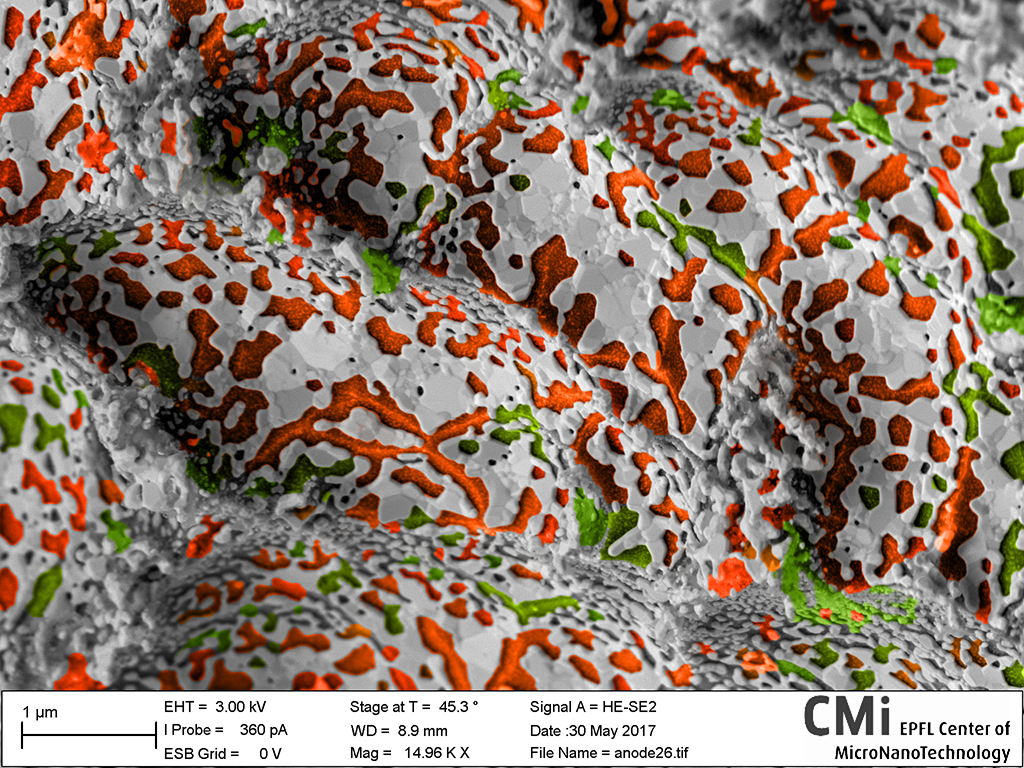
Valuable Red Lichen
Mahmoud Hadad, LC
The lichens are surprisingly very valuable, they have similar properties to Pt which can be an outstanding discovery in semiconductor industry. The recipe is very simple, try to deposit Pt on tiny opening through silicon wafer.
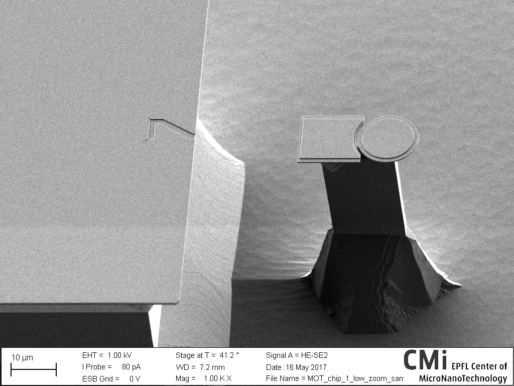
Enterprise (NX-01)
Ehsan Mansouri, Ryan Schilling, LPQM
This image shows a high resolution SEM image of a novel optical microdisk with an outside trench and also a corresponding supporting stage to place 2D materials in the vicinity of a microdisk resonator electrical field which can improve the optical properties of the bare microdisk. The disk and its supporting stage are made out of glass (silicon oxide) and the pillars underneath are silicon. For this structure we use two aligned ebeam lithography masks, one photolithography mask, SPTS, AMS and KOH. It looks more like a starship Enterprise in Star Trek than an optical resonator.
2017, April
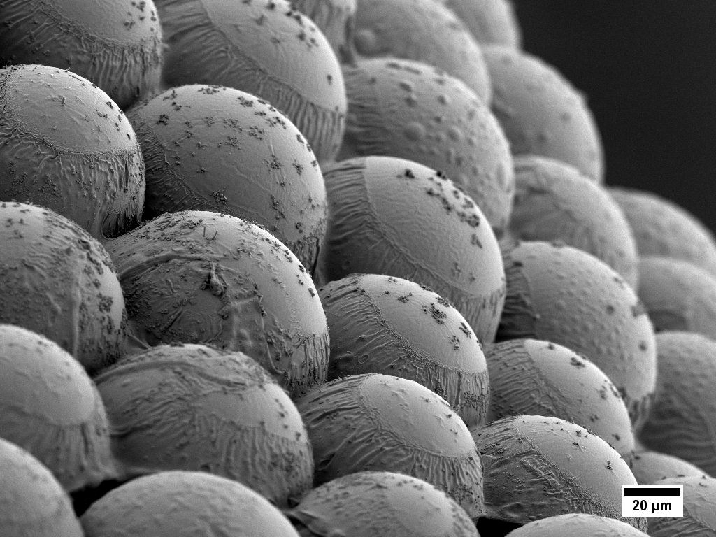
Resting jellyfish
Michael David Kessler, SMAL
“Bunch of jellyfish having a rest on the sea ground.” The picture shows a hydrogel sheet containing PEG particles that are held together by alginate. The stripes on the sides of the particles is alginate, backfilling the empty space between the particles. The little pieces on the top of the particles is probably CaCl2 that was used to gel the alginate. They can be seen as little parasites sitting on the jellyfish. We are fabricating the microfluidic PDMS devices in CMi (zone 12), as well as the wafers to make them (zone 13).
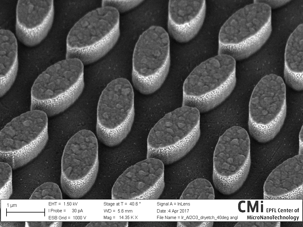
Easter Nano Eggs
Aleksandrs Leitis, BIOS
Easter nanoeggs brought to you by Easter nanobunny from CMI. Unfortunately the Easter nanobunny was too nimble to get captured by the SEM. Let’s hope for better luck next Year!
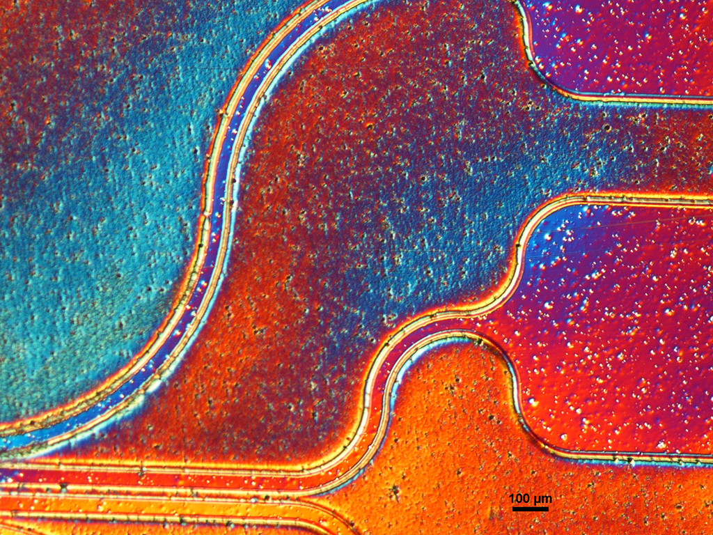
Golden tracks
Celine Fischer, Phil-Dominik Simon Reukauf, Jarla Thiesbrummel, LSBI
This picture was taken in the context of the “Lab in tube” competition, supervised by Stephanie Lacour’s lab. This is part of a resistance temperature detector design proposed by our team. The surface is only gold and the pattern one can see is part of the tracks linking the sensor itself to the connector pads. The picture was taken after the metalization step. The design was obtained thanks to photolithography on a flexible substrate (polyimide). All the steps were performed at CMI (lamination, exposure, development, metallization and lift-off).
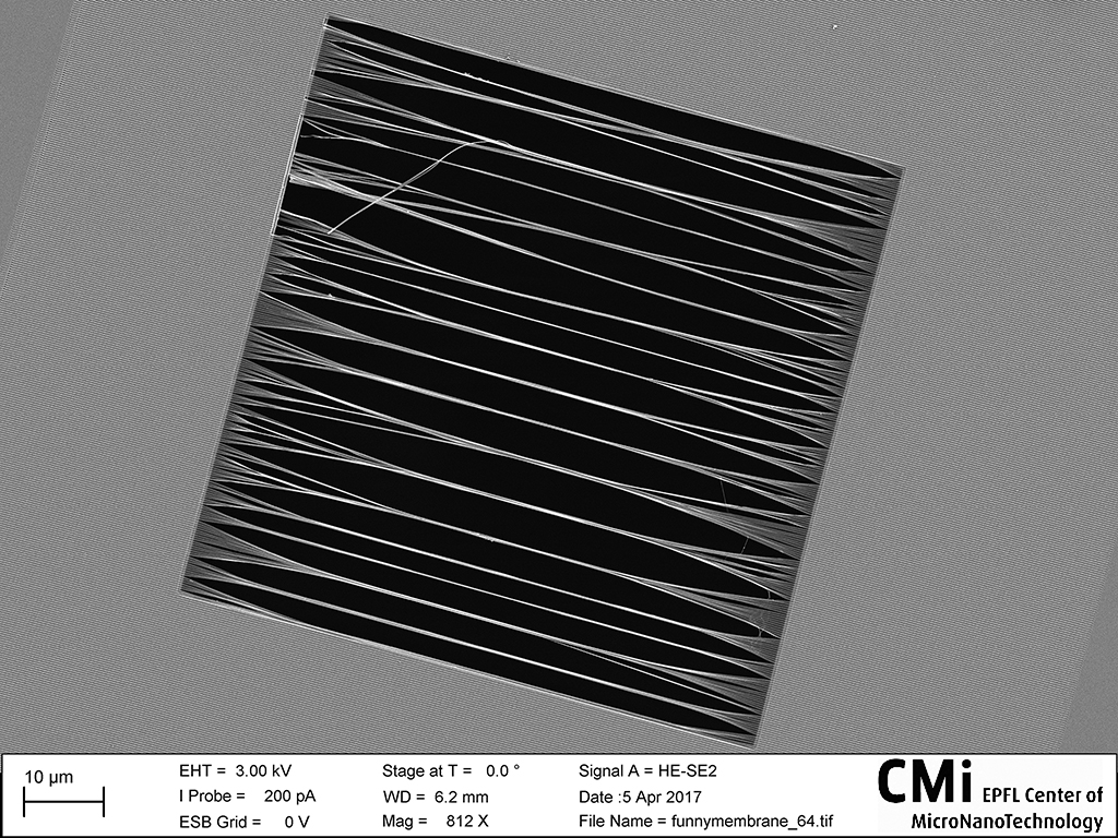
Weaving Silicon Nitride
Michael Graf , LBEN
Potassium hydroxide silicon etching was used to create a 30nm thick silicon nitride membranes. E-beam lithography and reactive ion etching (RIE) are used to make tiny holes into this membrane. The SEM mode of an electron beam lithography system was used to align the wafer using one of the etched membrane. After the RIE step, 200nm wide and 30nm thick bands of freestanding silicon nitride are observed. This is due to scanning the area with electrodes. The individual threads of silicon nitride arrange themselves into twisted bundles forming strings spanning the whole membrane.
2017, March

Stars
Benoît Desbiolles, Arnaud Buxtorf, LMIS4
The local sputtering of the photoresist sidewalls is actually useful if you want to fabricate micro-stars with a 50nm thin nano-wall using standard photolithography tools. 100% Made in CMi.
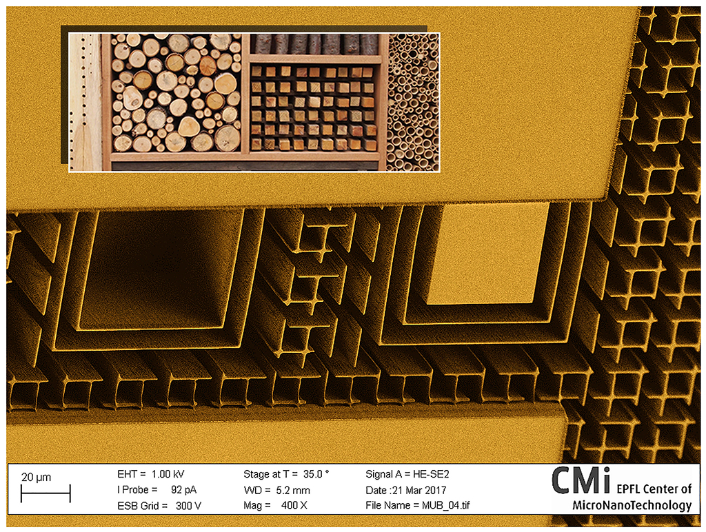
Silicon Nano Insect Hotel
Junqiu Liu, Tiago Morais LPQM
The “hotel” was fabricated using Alcatel AMS 200 SE dry etcher. Due to insufficient oxide etching on the previous step, the residual oxide served as a hard mask for the Bosch process deep silicon etch. The result is these high aspect ratio -1µm thick, 150µm high- walls with the typical edge roughness of a Bosch process. The hashtag pattern builds isolated box spaces, which look pretty like an insect hotel. Insert image by Emily Manley, used with her permission.
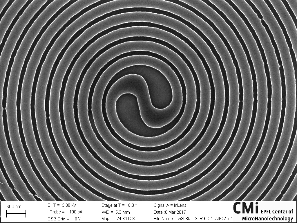
Single photon detector
Misael Caloz, GAP Quantum Technologies
Molybdenum silicide superconducting nanowire single photon detector. When cold down to below 1K, the nanowire becomes superconducting. A telecom photon has a very high probability to be absorbed in it, if it does it will break a Cooper pair and destroy the superconductivity, an electric signal can thus be recorded with a readout circuit. This device can have efficiency higher than 90%, with a repetition rate of tens of Mhz. We are now testing this original double spiral design, as it can cover a large area (high fill factor) with only two short turns (in the center). Such devices are directly used in our lab in Geneva, for quantum experiment such as QKD and quantum teleportation. In the latter case we could call this nanowire a “quantum portal”, as it can teleport the quantum state of a photon. Fabricated and imaged in CMi.
2017, February
Earthquake
Clemens Herkommer, Junqiu Liu, Mohammad Bereyhi LPQM
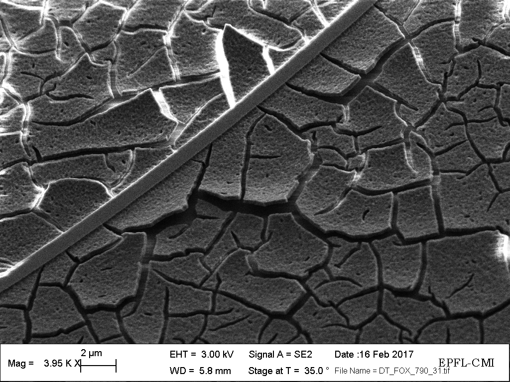
This SEM picture shows the surface of a silicon wafer with a layer of FOx ebeam resist peeling off after development. A written line can be seen as a solid structure embedded in an unexposed area that was not cleared due to a low contrast. Electron impingement during SEM imaging caused the flakes to charge up and delaminate from the wafer surface. On a micrometer-scale, this looks like the open earth crust after a heavy earthquake, with a pavement left over.
2017, January
Tie-Dye E-beam Sample
Martin Friedl, LMSC
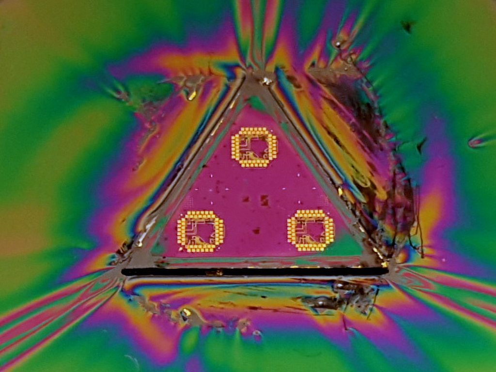
In the process of making contacts to (111)B GaAs triangular chips, I was impressed by this pattern that came out of the spin-coater. This psychedelic pattern is caused by the relief on the e-beam sample, namely, the raised triangular chip stuck with Indium on the flat square silicon dummy. This colorful pattern actually means the PMMA/MMA resist stack is non-uniform in thickness, however, you will notice the GaAs triangle itself has a uniform coating, which is really all that matters!
Array of super nova
Stefano Varricchio, LMIS4
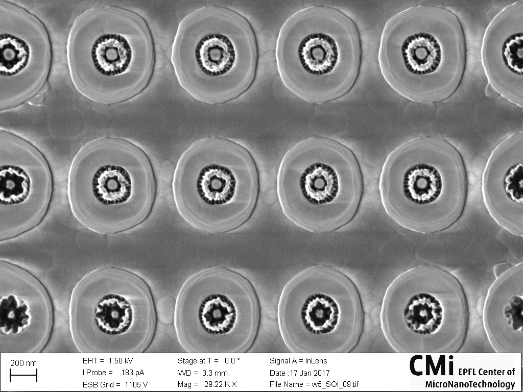
Nanostructured silicon embedded in amorphous carbon and silicon dioxide surface after planarization. Or you can think about them as timeframes of a huge supernova captured with a space telescope.

“U” structure
Luka Ciric, LPMC
Focused Ion Beam was employed to cut a lamella out from a layered material and to shape it according to the “U” structure. Suchconfiguration allows for the simultaneous measurement of the electrical resistivity along the different crystallographic direction of the sample. It represents a very reliable method to estimate the electronic anisotropy of a material relevant for electronic applications.