Back to the current year Winners
2018, December
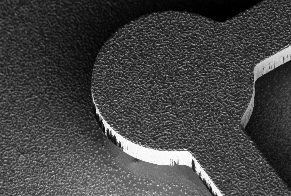
Rain on my wafer
Hernan Fernando Furci, CERN
After having released a 5-micron thick SiO2 structure, supported by pillars sculpted from the Si substrate, raindrops (of Au and Sn) fell on mi wafer, projecting dry shadows on the remainder of the substrate (which lies 8 microns beneath the SiO2) right under the released pattern.
2018, November
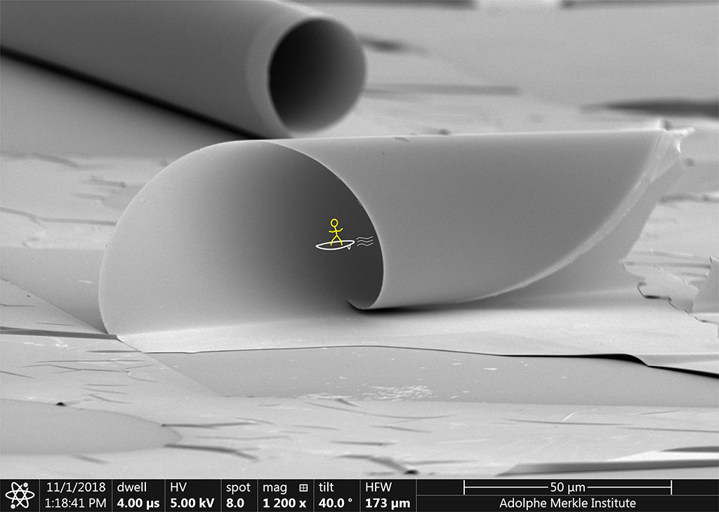
Half-pipe wave
Esteban Bermudez Ureña, Soft Matter Physics, AMI
With the cold winter season approaching, many CMi users will be dreaming of escaping the cleanroom to some tropical paradise. However, the perfect half-pipe waves might be closer (and smaller) than you think. The image shows a self-rolled SiO2/Au bilayer film that suffered some defects along the way, creating a curious breaking wave-like 3D shape. The substrate patterning (MLA150) and thin film deposition (LAB600H & SPIDER) were carried out at the CMi. The roll-up process and SEM imaging were performed at the Adolphe Merkle Institute in Fribourg.
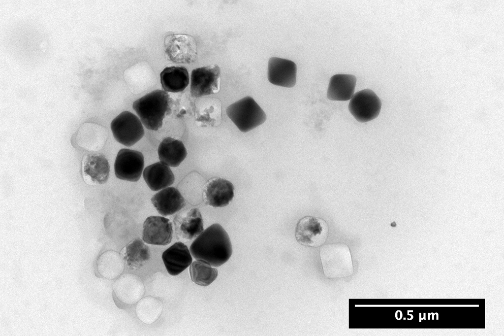
Octahedral copper electro-catalyst after work
Jan Vavra, INE
Some particles survived without a scratch, others left only their shadow behind and some are on their way to complete destruction. Picture was taken on the Osiris TEM of CIME, and the electron transparent sample support, 50 nm SiNx with 18 nm glassy carbon was fabricated in the CMi cleanrooms.
2018, October
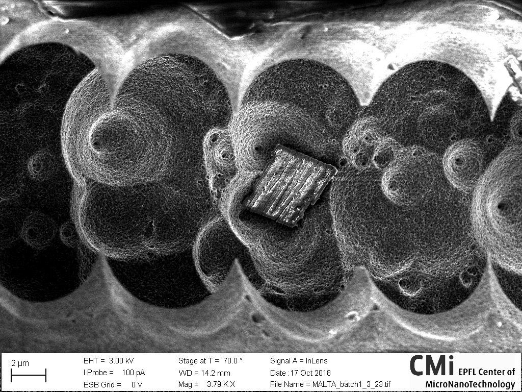
A window over the world of magic
Riccardo Callegari, CERN
Need to get inspired for your next abstract painting? Let the XeF2 do his job and just copy that. What you are looking at is the bottom of a microchannel, etched by XeF2, seen from an opening in the overlying silicon. The entire fabrication has been done with the CMi equipment and the picture has been taken with the MERLIN.
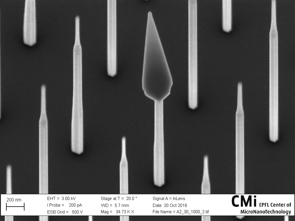
Let there be light…
Akshay Balgarkashi, LMSC
This GaAs nanowire chooses to lighten up and brighten the surroundings even as the others choose not to, just as we are here not to curse the darkness but to light up the candle leading us to a technologically bright future. These vertically standing quantum thin nanoneedles on patterned silicon substrates are grown by molecular beam epitaxy on top of GaAs nanowires just by varying the As flux during growth.
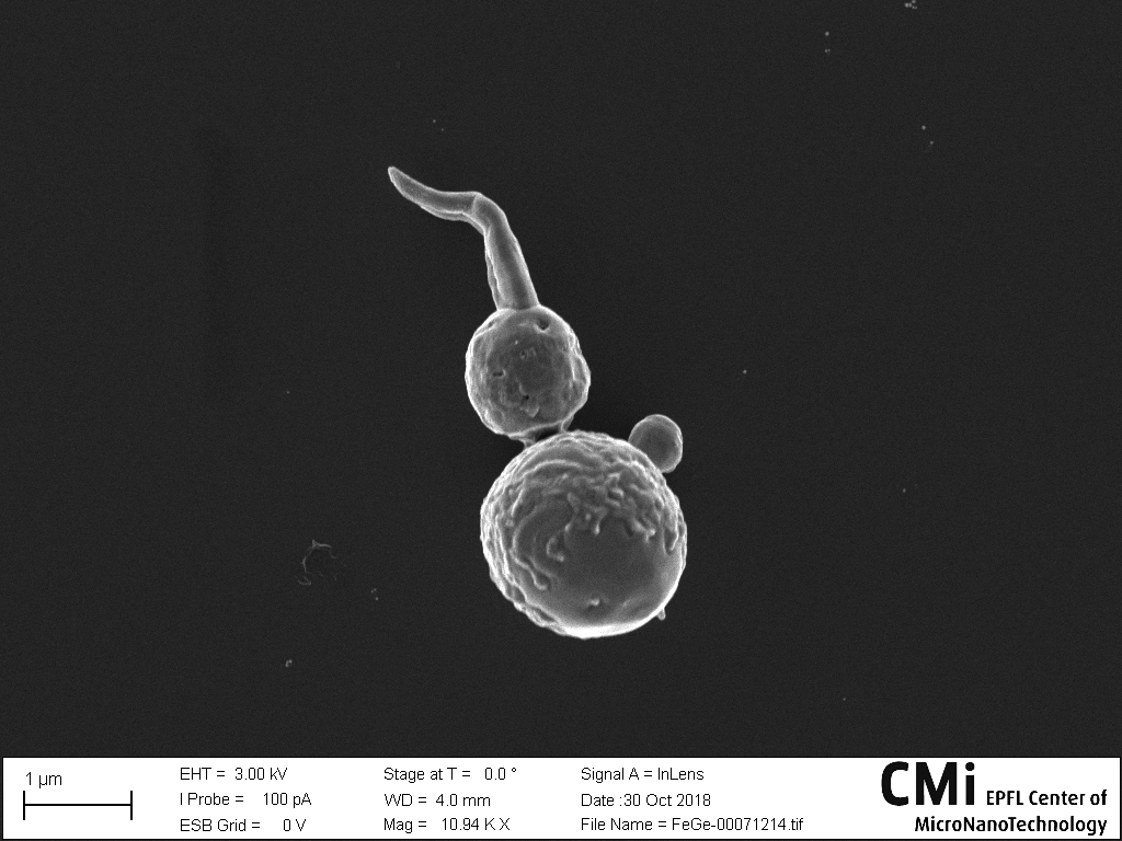
Winter is coming!
Tzu-chin Chang Chien, LMSC
An iron snowman accidentally fell down on the silicon wafer, making its nose crooked, ouch! The winter is coming!
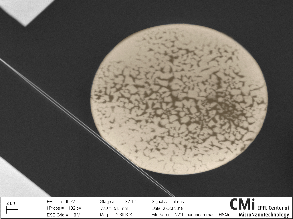
Full moon
Mohammadjafar Bereyhi, LPQM
Full moon appears on a chip to brighten its darkest night… This is a picture of a silicon dioxide micro-disk that has different thickness compared to the adjacent rectangular pads (visible in corners of the picture), it has been filled with poly-silicon as a sacrificial layer and polished using CMP. After that a nanobeam made of silicon nitride is patterned on top of the flat surface and patterned with electron beam using HSQ. In this picture the CMP process did not work very well on this region of the wafer so the surface of the disk is not well-polished and as a result it looks like patterns that exist on the moon.
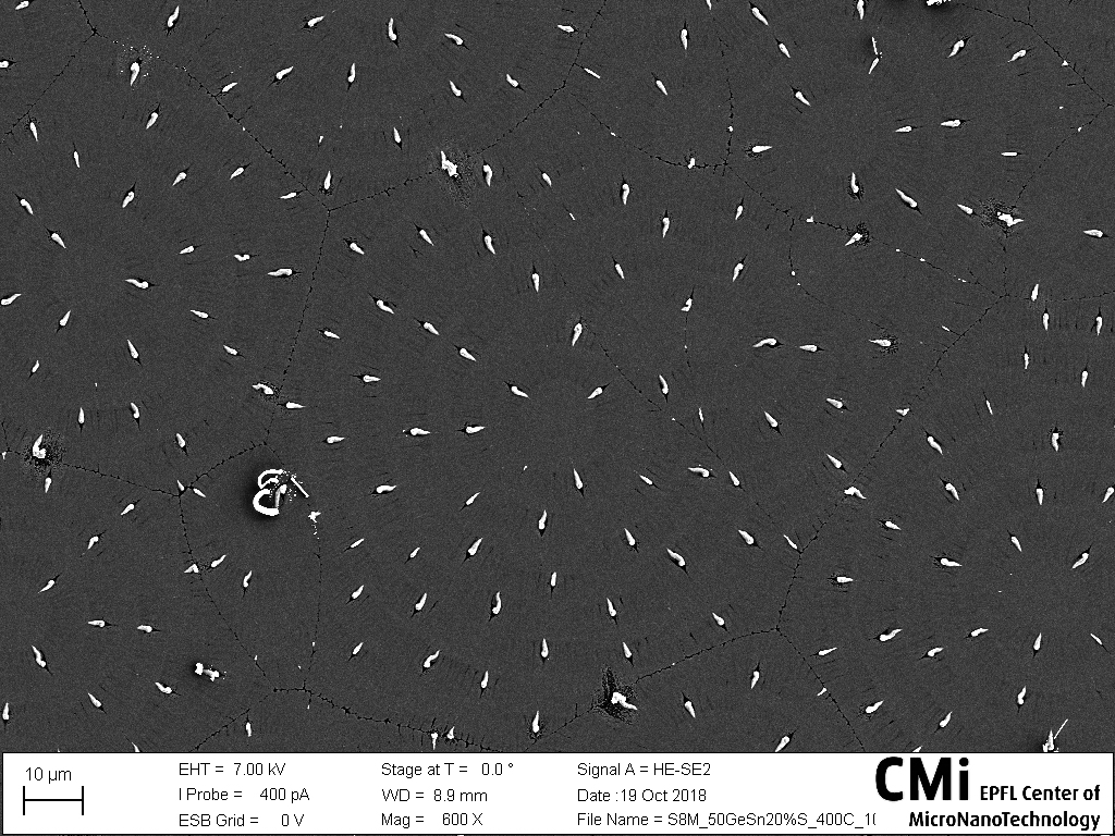
Worm Attack
Marcelo Alejandro González Alanís, LMSC
These worms, rich in Ge, were created by rapid thermal annealing at 300 °C for only 10 seconds on a sputtered Ge0.8Sn0.2 thin film (50nm). But beware, they know Halloween is coming and they are hungry for any type of candy you might leave forgotten on your desk.
Mind the nano-gap!
Maneesha Rupakula, NANOLAB
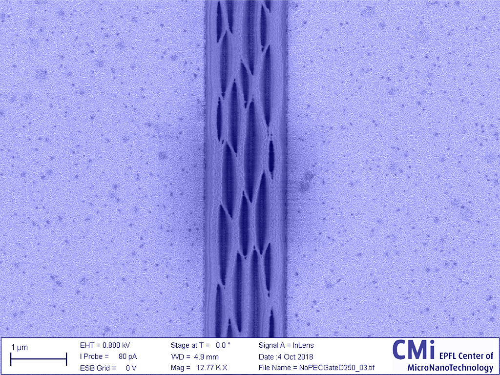
A word of caution for adventurous hikers: You are strongly advised to watch out for crevasses also in the Aletsch glacier of the miniature world. Do familiarize yourself with the rescue procedures before proceeding! In other words, you are looking at a tall (Aspect ratio = W:H = 1:6) of collapsed 50nm line and space pattern in ARN resist after development.
Happy Halloween!
Chao Liu, Powerlab
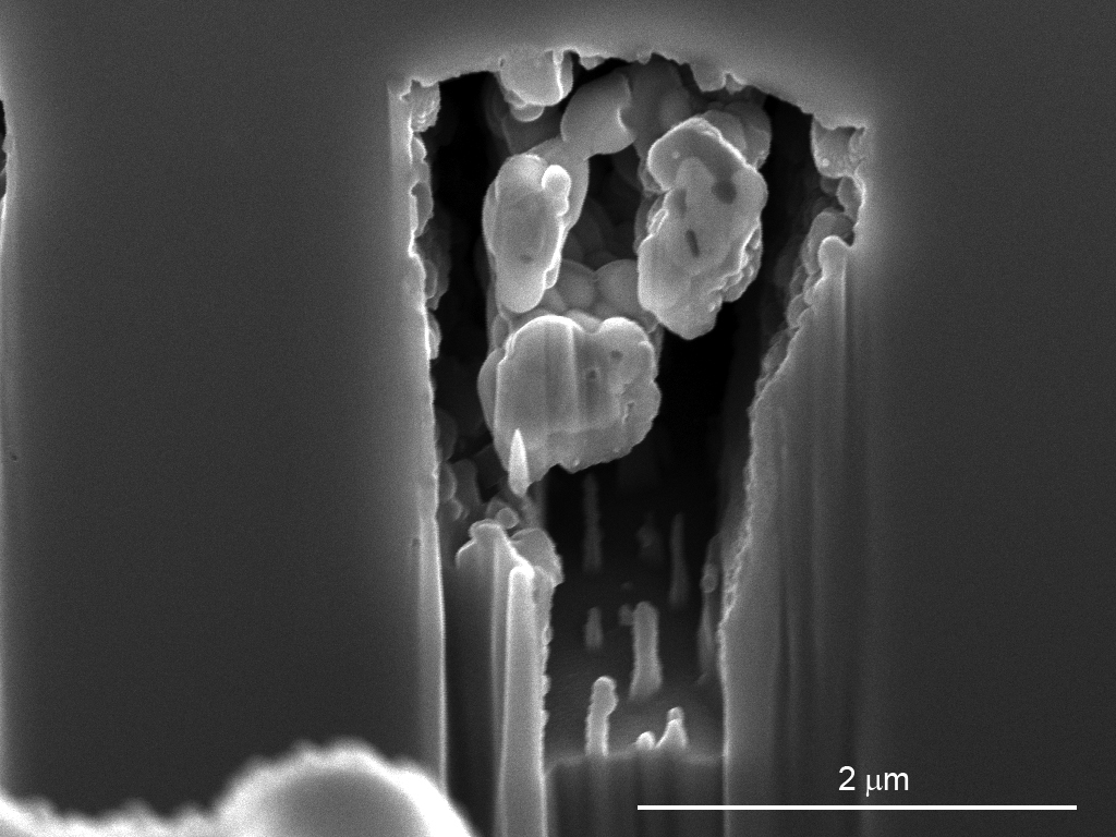
I found this little angry ghost hidden in my GaN crystal on the day of Halloween. It was created unconsciously by catalyst-assisted GaN decomposition at high temperature and captured by SEM after a FIB cut.
2018, September

Micro-Iron throne at the edge of the world
William Courbat, LMIS4
Characters from Game Of Thrones were tired of sitting in the dark room of the throne, so they moved it at the end of a cantilever to appreciate the view and the fresh air. This Silicon Micro-Throne is the result of contaminants during a Bosch process. Particles masked parts of the wafer leading to these long structures. It now sits on a 2um thick, 50um wide and 350um long AFM cantilever.

Parylene leaf
Riccardo Callegari, CERN
Also the parylene leaves in autumn begin to wither.
From the bottom to the skies, love is the essence.
Amin Hodaei, SMaL
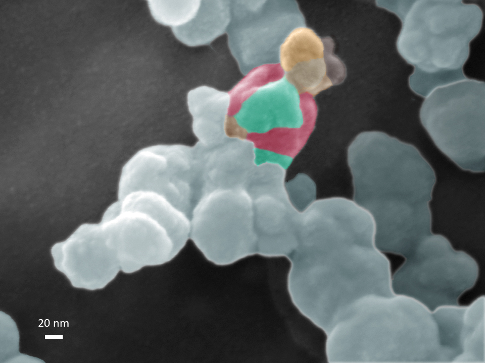
Floating on the clouds, at the bottom of the matter, two lovers united. These lovers are made up of calcium carbonate nanoparticles which have been synthesized using a microfluidic spray-drier fabricated at CMi.
Les Triangles
Rajrupa Paul, LMSC
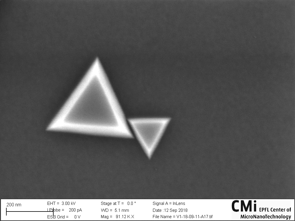
Zn3P2 nano-triangles grown on graphene using MBE.
2018, August
Fire, full moon
Mohammad Bereyhi, LPQM
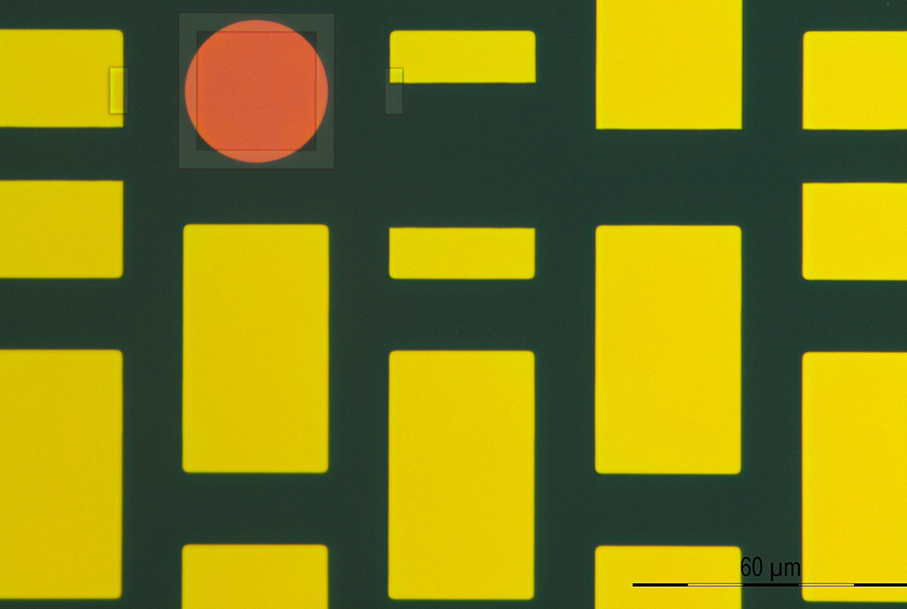
This is an optical image of silicon oxide patterns on silicon. The circle is going to be an optical microdisk resonator and it has a different thickness than the surrounding pads, that is why it has a different color. It has been planarized using Poly-Si sacrificial layer and chemical mechanical polishing (CMP). The square pattern on the circle is an HSQ mask written with ebeam in order to calibrate the possible offset of the circle and rectangular pads from the original mask. This can happen due to nonlinear and possible anisotropic etching nature of BH. This picture resembles an artwork by Paul Klee, a Swiss-German artist from 1930s, called “Fire, full moon”.
Heartwarming love
Mojtaba Rezaei, LAS
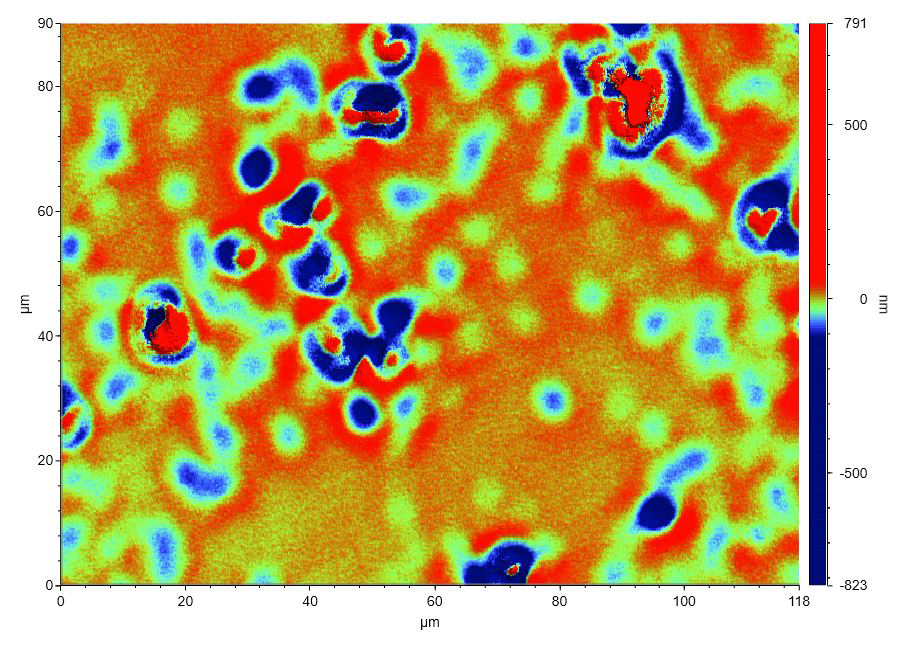
Optical profilometry image of the surface of an epitaxially grown Cu(111) on a sapphire substrate. Although not achieving the desired smooth surface this time, the heartwarming love in the upper right corner of the image keeps you motivated and happy to continue optimizing the synthesis; knowing that the materials you synthesize appreciate your work and show you their love and support!
Shattered Dreams
Sebastian James Davis, LBEN
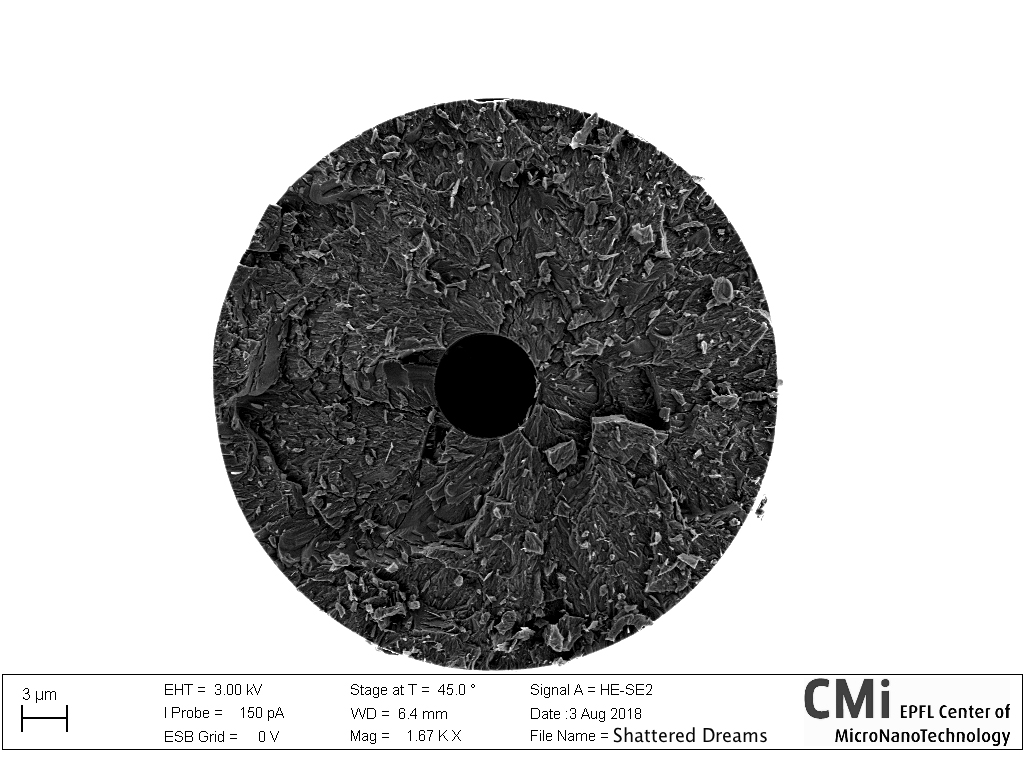
You expect to see a perfectly conical glass nanocapillary. Instead all you get is a callback to an 80’s pop song… nothing but shattered dreams, shattered dreams. Feel like I could run away, run away. From this PhD. (apologies for the bad singing) Unfortunately, while inspecting pulled glass nanocapillaries that should be ~50nm in size, it becomes glaringly obvious when a handling mistake has been made, and a capillary broken.
2018, July
Deux étoiles…
Benoît Desbiolles, LMIS4
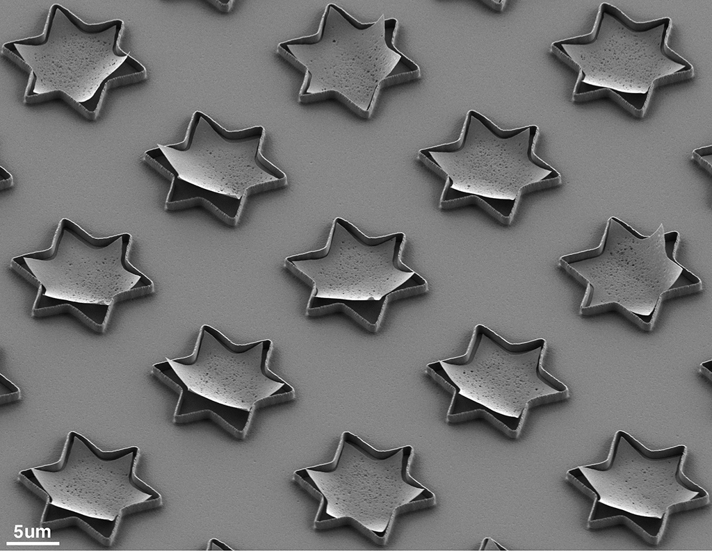
Scanning electron microscope image of star-shaped silicon nano-patterns standing on a glass substrate. A thin membrane of stressed silicon can be observed in the structure. This was simply done by combining standard photo-lithography with ion beam etching. 100% Made in CMi.
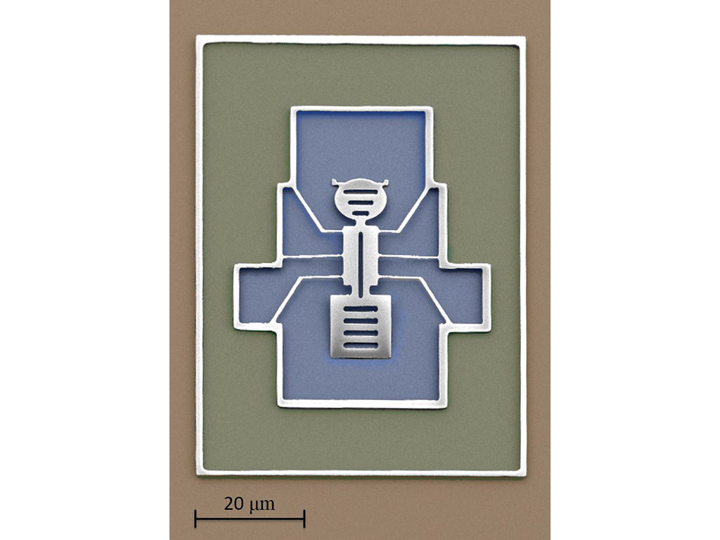
Micro-ant’s summertime
Hamed Sattari, Q-Lab
This lucky poly-silicon ant rests over its 1um deep fancy swimming pool, these hot days! It should be thankful of a clean HF vapor release process. For creating this micro-ant and its swimming pool, starting from a silicon wafer with 1um wet oxide layer, we first dry-etched the oxide down to the handling silicon layer (green area). Afterwards, a 100nm thick LPCVD poly-silicon layer became deposited over the wafer. Next, we patterned the ant using full dry etching of the poly-silicon layer. The VPG direct laser writer has been used for the lithography steps. Finally, we fully released the ant using HF vapor release process, which removed all the 1um thick oxide inside the puddle and under the ant.
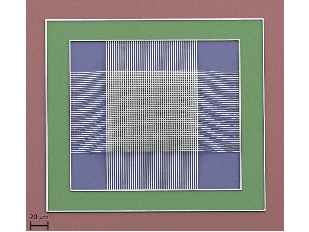
The trampoline over the swimming pool
Hamed Sattari, Q-Lab
We have all the facilities prepared for you down here on our chip. Just come here and enjoy your summer at CMi! To fabricate this structure first we had to dry-etch fully 1um of wet oxide down to the handling silicon layer (green area). Afterwards, a 100nm thick LPCVD poly-silicon layer became deposited over the wafer. Next, we patterned the trampoline using full dry etching of the poly-silicon layer. The VPG direct laser writer has been used for the lithography steps. Finally, we fully released the structure using HF vapor release process, which removed all the 1um thick oxide inside the swimming pool and under the net.
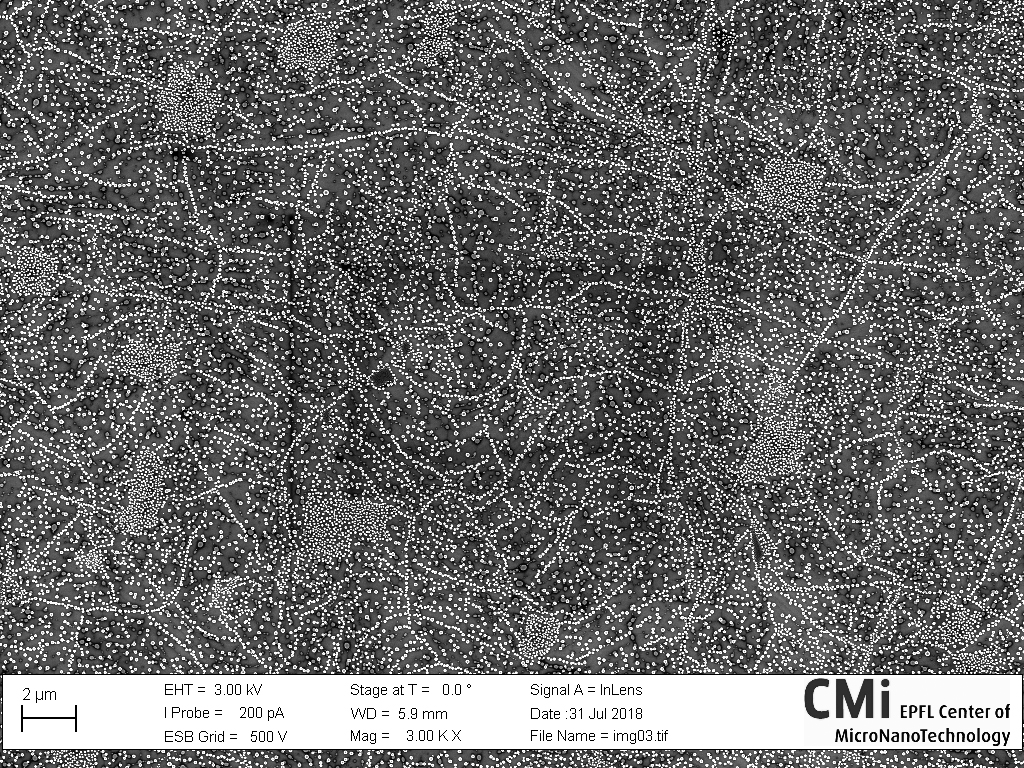
Graphene Galaxy
Akshay Balgarkashi, LMSC
Revealing the observable universe of graphene. These Ga droplets arrange themselves like planets, stars and galaxies along the grain boundaries and cracks on a monolayer of graphene revealing a galaxy not so far from us.
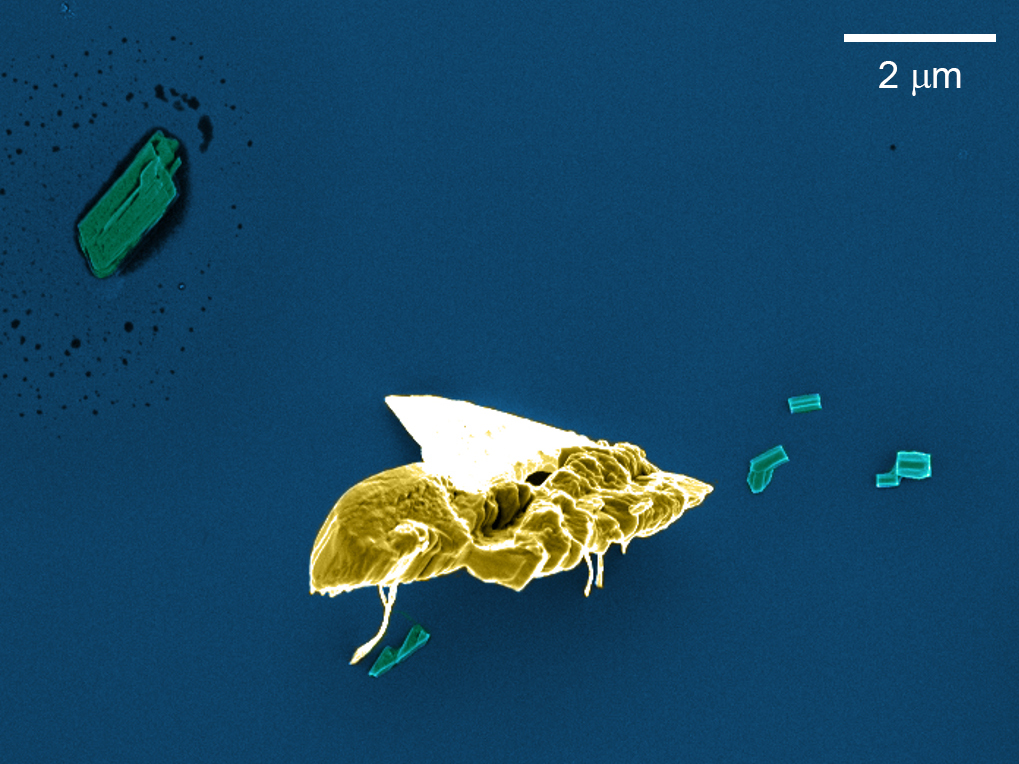
Hungry Crystal Fly
Aysu Ceren Okur, SMaL
I found this little one eating up my crystals to grow! Micron sized calcium succinate crystals were obtained upon drying of aerosol that are generated through surface acoustic waves. Interdigitating transducer electrodes on piezoelectric substrate which produces surface acoustic waves were fabricated in CMI.
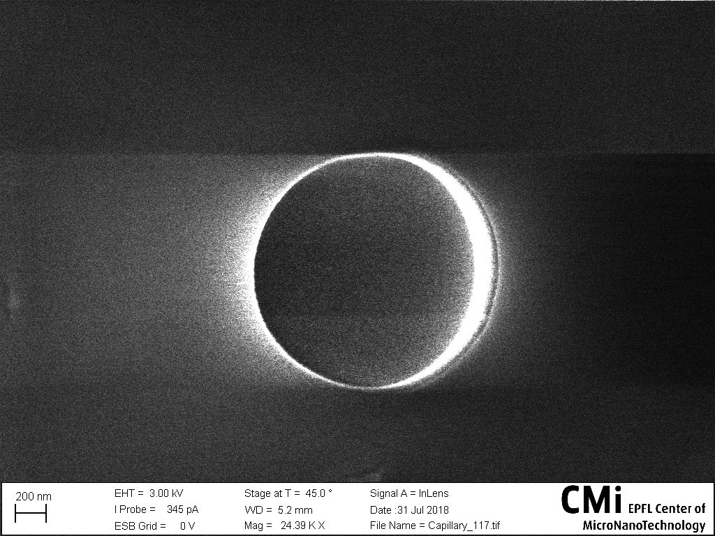
Lunar Eclipse
Mahdi Sahafi, LBEN
The second total lunar eclipse of 2018 was visible in large parts of Australia, Asia, Africa, Europe, and South America. It is the longest eclipse of the 21st century. If you lost it, you can come to CMi and see it again…. WAIT! … In fact, it is a top-side image of a glass nano-capillary under Merlin SEM, built for the detection of the DNA translocations.
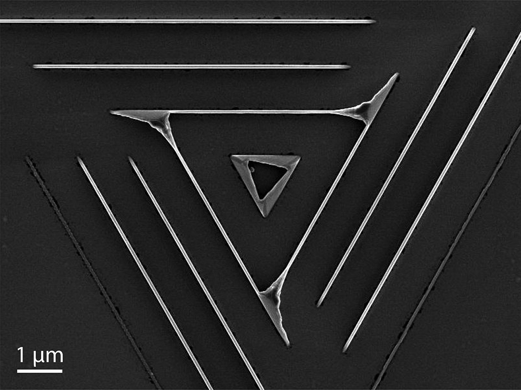
MBE Ninjas
Martin Friedl, LMSC
Oh no! Those pesky MBE Ninjas have infiltrated our lab and started operating our molecular beam epitaxy chamber to produce their shurikens! Though you have to give them credit, they are using the ingenious approach of selective area epitaxy. Here, a SiO2 mask limits the growth of GaAs membranes to specific lines oriented on a GaAs substrate to achieve the desired pattern. Maybe these structures could also be useful for quantum transport experiments… Hmm, we should try that!
2018, June
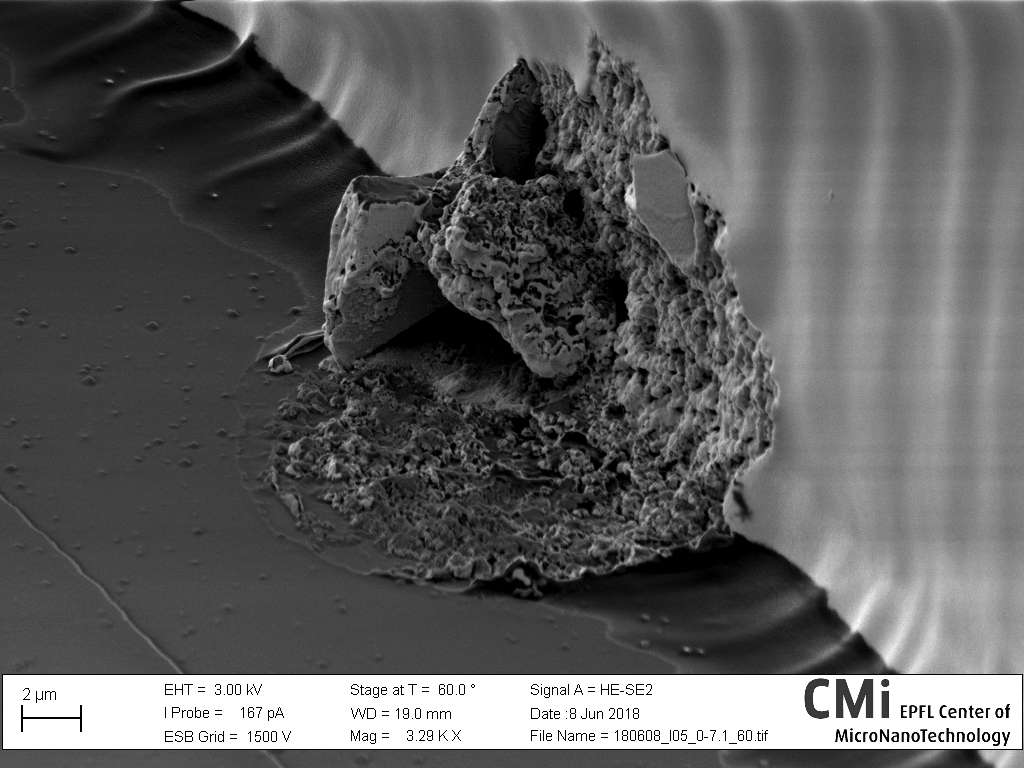
Nano coral reef
Kevin Keim, CLSE
This nano coral reef appeared after metal coating and ion beam etching of our three dimensional electrodes. In the background one can see SU-8 dunes and rocks of remaining platinum.
2018, May
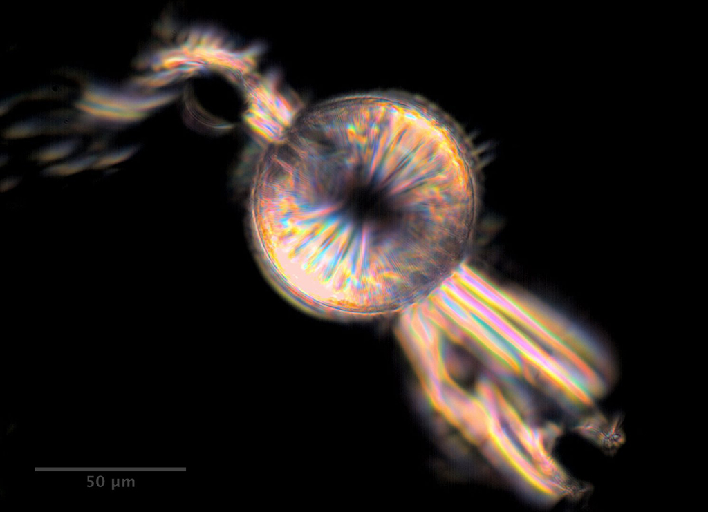
The Eye of Sauron
Matthias Neuenschwander, LBNI
Top view of Barad-Dûr, showing the ever-watchful eye of Sauron, suspended between the two peaks of his tower in Mordor. In reality, this is an optical microscope image and was taken in dark field mode. The two ‘peaks’ are SU8 pillars, whereas the eye is an (accidental) bubble in a sacrificial layer.
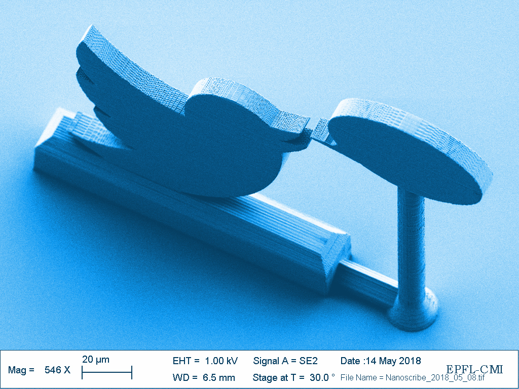
Micro Twitter Bird
Lorenz Hagelüken, LMIS1
This sweet mountain bluebird was procreated in the Nanoscribe Professional GT by NIR photons interacting with a drop of IP-Dip resist. After graftage with an 18 nm gold coating (DP 650), it has been released for its first flight in the Zeiss LEO 1550’s vacuum chamber. Its raison d’être is just to spread good news to the world
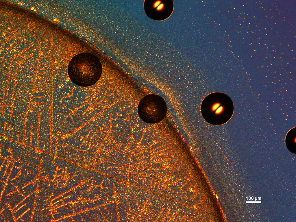
Not stars and space
Ahmed Aqeel, LQNO
Nanoparticles dropcasted to a flat gold surface with hemispherical holes irradiated in BF microscope.
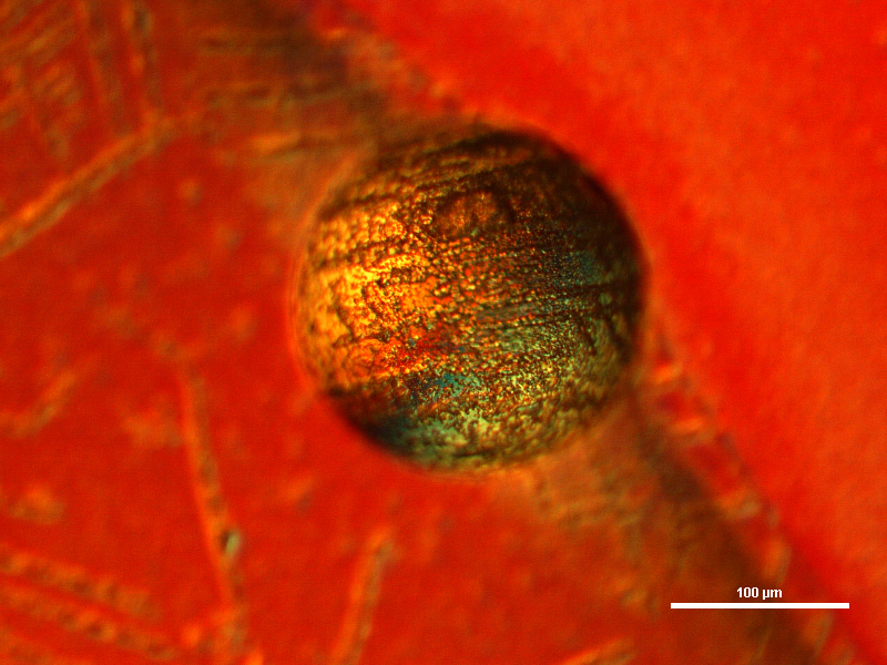
Death Star
Ahmed Aqeel, LQNO
AuNPs in a hemispherical hole in flat gold….Looks a lot like death star.
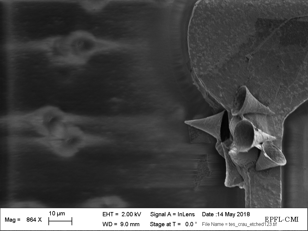
Ice-cream cone factory
Ece Ozelci, CERN Cryolab
A tiny ice-cream cone factory has been launched on our Transition Edge Sensor’s delaminated Cr/Au coating.
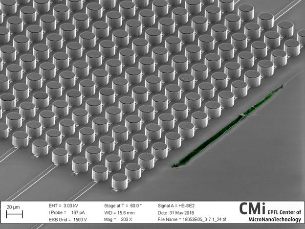
Snake in DLD labyrinth
Kevin Keim, CLSE
This snake left its platinum skin in front of this deterministic lateral displacement (DLD) labyrinth out of metal covered SU-8 posts. Is it large enough after its shedding to get straight through the labyrinth or will it get displaced by a magic dielectrophoretic force hidden in the labyrinth?
2018, April
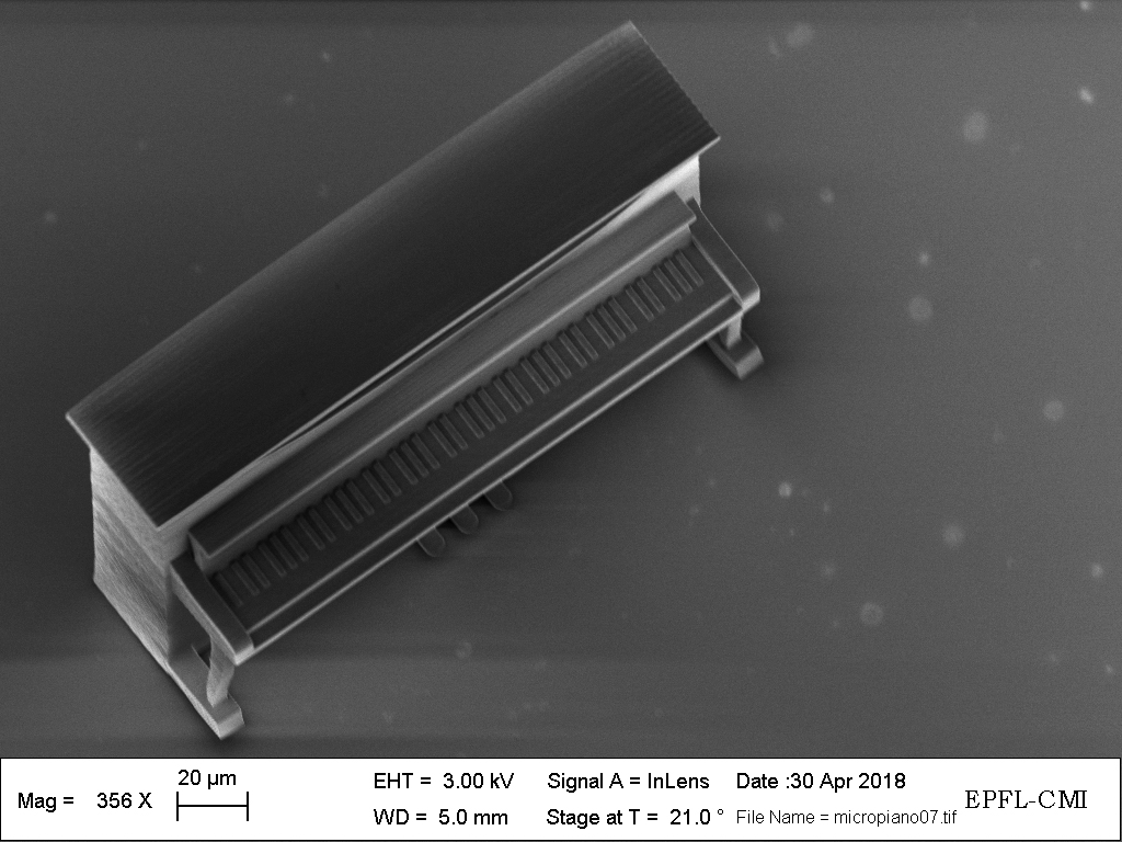
µ-piano
Giulia Panusa, LO
One day I was working late in CMi and suddenly I heard some music coming from somewhere. I decided to follow the music and I ended up in front of the Zeiss LEO in Zone 1. Therefore I peeked inside and with surprise I found a µ-piano!!!! This 3D model was fabricated by means of two-photon polymerization with the new Nanoscribe 3D printer in a polymer photoresist and in a dip-in objective configuration. The µ-piano is about 50 µm high and was written in less than one hour. Let’s hope it plays again soon!
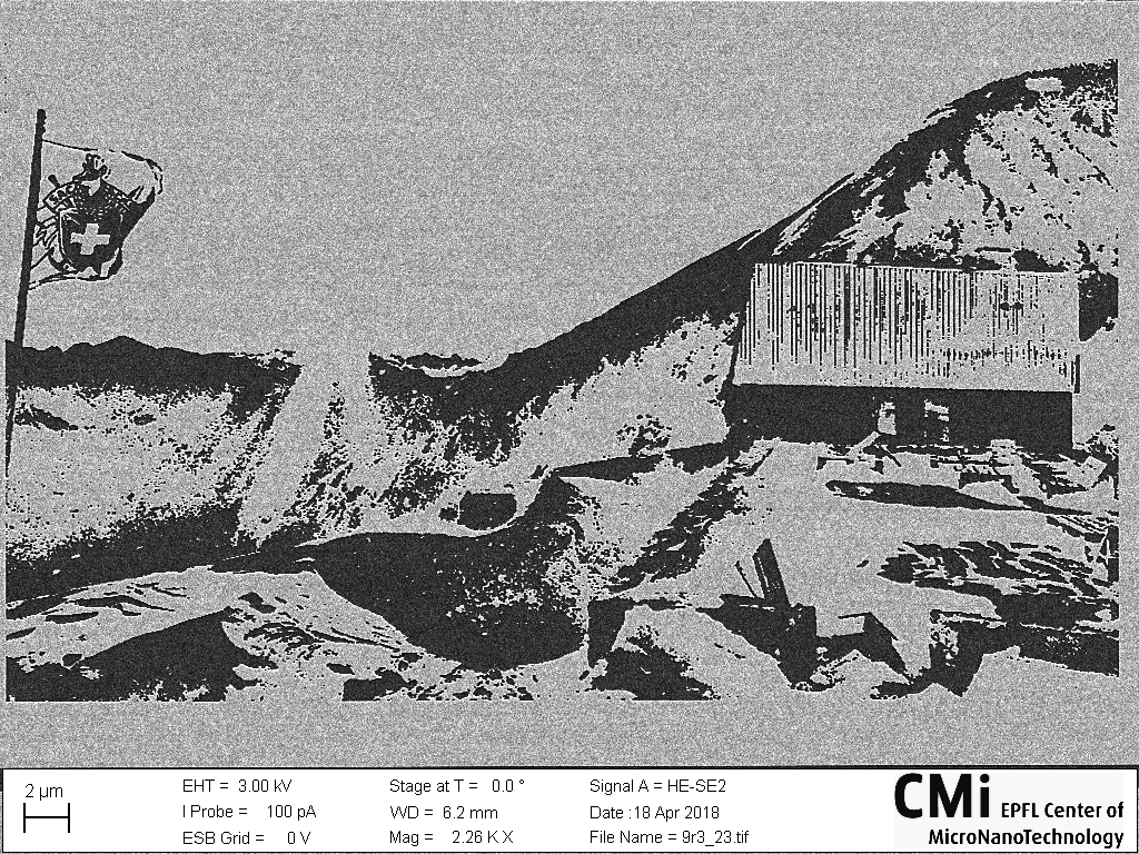
Tracuit mountain hut
Misael Caloz, GAP Quantum Technologies
This is what happens when you do to many e-beam sessions: at some point you get bored, start to think about why you started your PhD thesis or eventually you start to write a small python script that takes any .jpg image and transforms it into a gdsii file, you expose it on one of your wafers, etch it, and finally take a SEM image of it. The original photograph was taken by myself (also this month), it shows the Tracuit mountain hut (3256 m) in Valais, Switzerland the day I did the Bishorn ascension (4153m).
2018, March
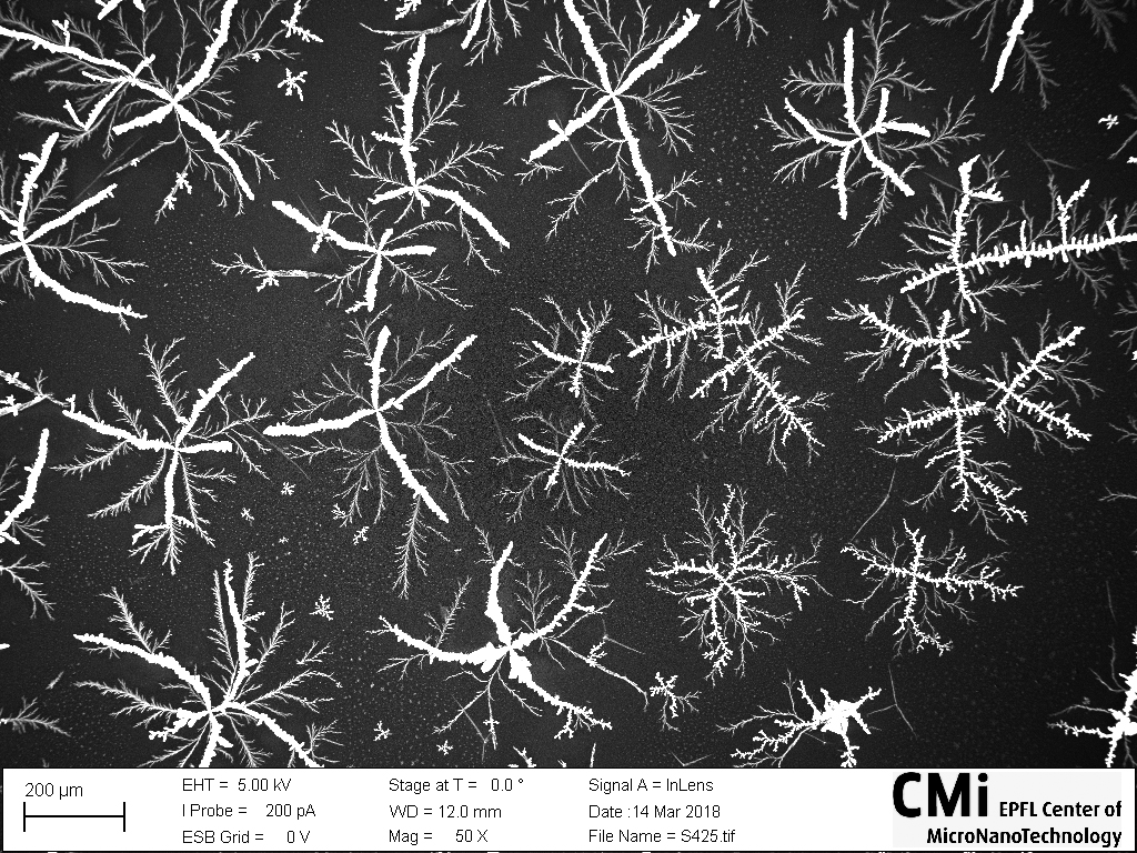
Nanomaze
Ahmed Aqeel, LQNO
To analyze their shape, 80nm diameter Au nanoparticles were dropcasted on template stripped Au substrates and left for evaporation. The particles seem to form eccentric maze like structures.
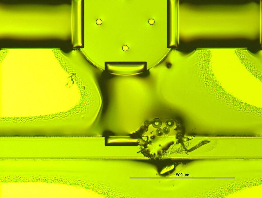
Fluffy guy, I’m gonna eat you!
Julia Tischler, LBNC
Cell culture chamber with pillars and flow channels patterned in SU-8 (30um high), with valves patterned in AZ (20um high), on Si-wafer. ‘Alien’ (top, middle) = cell culture chamber (alien’s head) with pillars (eyes & nose) and valves extending to the left & right (ears), mouth with huge tongue (valve, reflowed) below. ‘Fluffy guy’ = particle that has landed on the flow channel. Patterning and imaging performed at CMI.
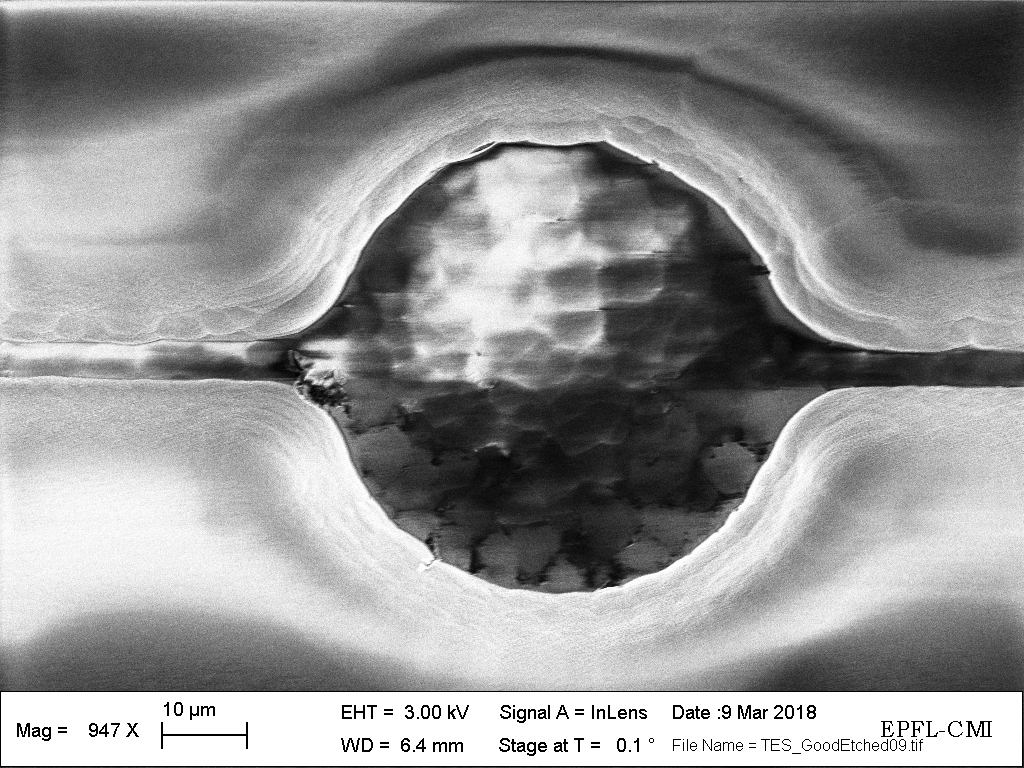
Micro-golf ball potential flow display
Hernan Fernando Furci, CERN
In this picture you can appreciate an artistic view of what the classical potential flow function of an inviscid fluid looks like around a microscopic golf ball. Technique: Delaminated-mask HF-etching on borofloat.
2018, February
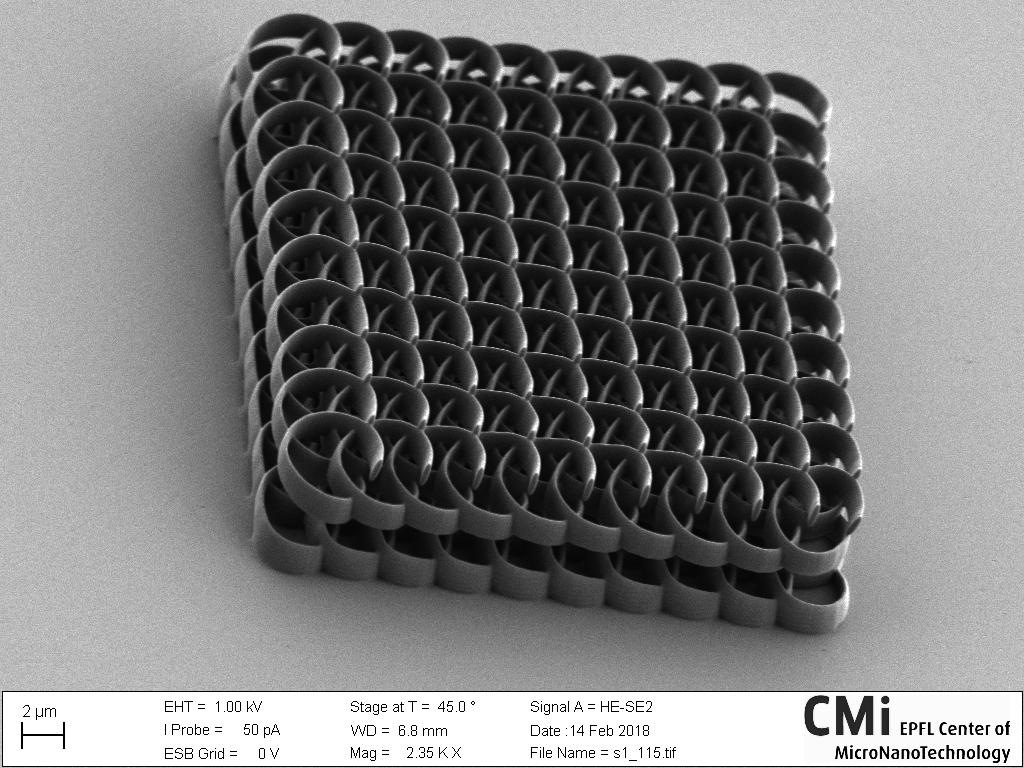
3D Helices
Julien Dorsaz, CMi
These 3D helices are printed with the Nanoscribe professional photonic GT using two-photon absorption mechanism, in piezoscanning mode. The voxel, i.e. 3D pixel, dimensions are 1 um in z-axis and 200nm in both x- and y-axis. Here the voxel follows a mathematically-defined 3D trajectory by scanning into the negative photoresist using the piezostage motors. This results in a very smooth surface.
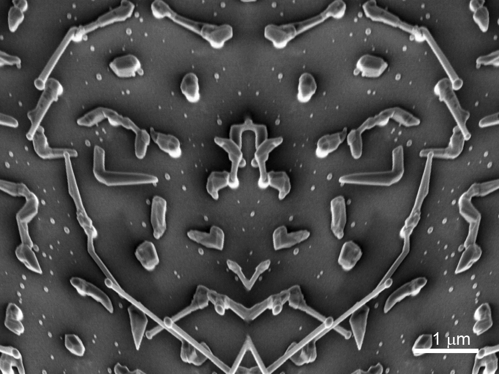
Valentine’s day with nanowires
Oscar Garcia, Lucas Guniat, LMSC
Mirrored image of GaAs nanowires grown on silicon pillars. The spirit of Valentine’s day is present in our sample, where nanowires seem to build the shape of a heart. Valentine’s day is meant to be spent with your true love, and so we did, having a date with our nanowires at LEO SEM.
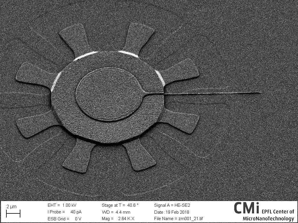
Heart of quantum electro-mechanical system
Amir Youssefi, LPQM
A star-like superconducting vacuum gap capacitor with a freestanding top plate made from Aluminium. This is the heart of every quantum electro-mechanical system.
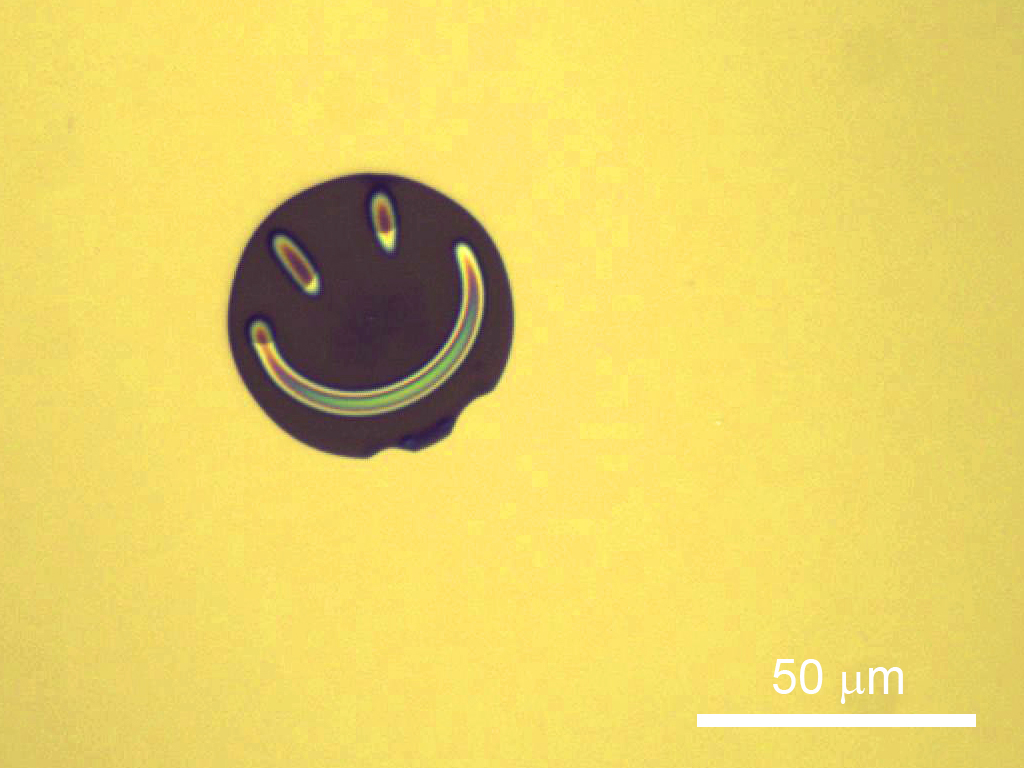
CMiley emoji
Esteban Bermudez Ureña, Soft Matter Physics, AMI
Underetching of a Ge layer with SiO2 on top. Upon drying, the SiO2 membrane attaches to the underlying Si substrate with some curious wrinkle shapes. Thin film depositions were carried out at the LAB600H and SPIDER systems. Underetching and optical microscope image performed at the Adolphe Merkle Institute in Fribourg.
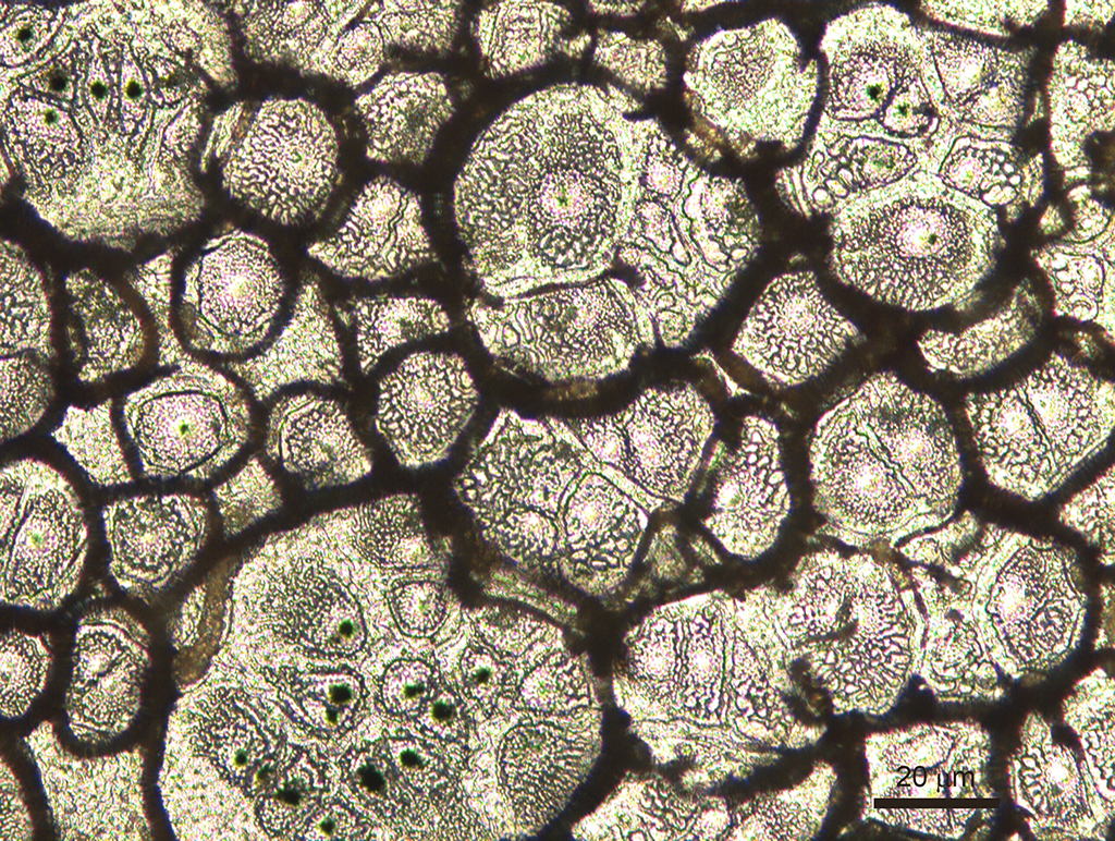
Flying over coral reefs
Hernan Fernando Furci, CERN
Air views of coral micro-reefs on an aluminium coated wafer. The topology is the result of overheated resin during an IBE process. The resulting bubbles and cracks interact with the optical microscope light and provide these beautiful landscapes.
2018, January
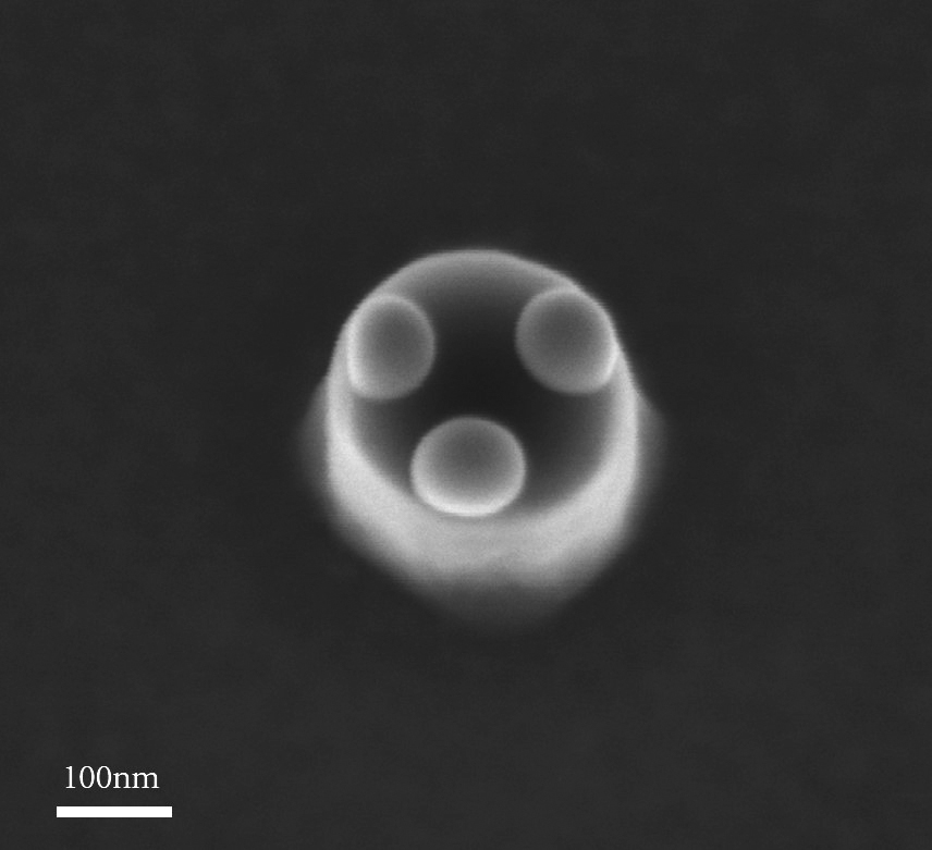
Zinc by MBE
Lucas Guniat, LMSC
“What a strange story is the one of our fluffy little friend. His body, made out of a 200 nanometer silicon pillar, was lacking arms and legs. In despair, not able to see or talk, he thought his life was programmed for an eternal darkness. But one day changed everything : This day where, after being introduced into an MBE chamber, he started seeing bright spots, fringes and pillars like him all around. “What a strange looking dream!” he then said. “I wonder if real life looks similar”. It took him 10 minutes at 730 degrees Celsius to realize he was not dreaming: Gallium condensation had given him eyes to see, and a mouth to talk. “I will never stop admiring the beauty of the world!”, he declared. Unfortunately, the temperature of the MBE going down, it would be harder and harder for him to move his lips and eyes, until reaching a point where his eyes wouldn’t blink. He was petrified, condemned to wear this horrible expression the rest of his existence, having no longer a voice to complain.”
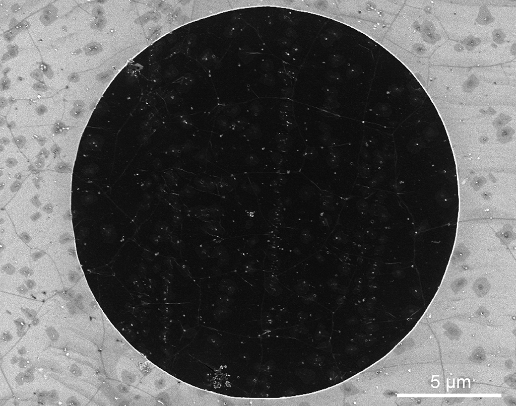
Grains of graphene
Tom Larsen, NEMS
Suspended sheet of CVD graphene. Grain boundaries and areas with multilayer graphene are clearly visible. Image taken using the SEM Merlin at CMi.
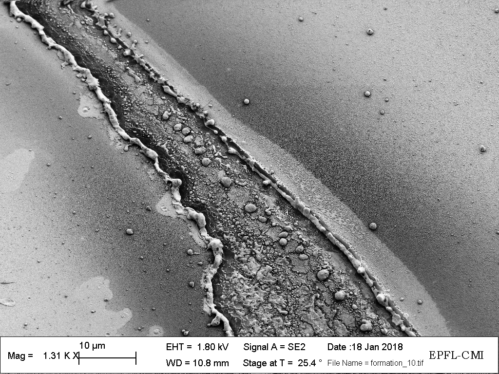
A valley on Mars
Mohammad Samizadeh, POWERLAB
It looks like a valley in a plateau. Maybe on Mars! But this valley is made after a huge number of sparks in a micro-plasma device on a chip! The concept is similar to ion beam etching. In each spark we make electrons as well as ions. The heavy ions are accelerated toward the gold electrode and etch it! One can say that it is an on-chip etcher. Picture is taken after one thousand sparks.
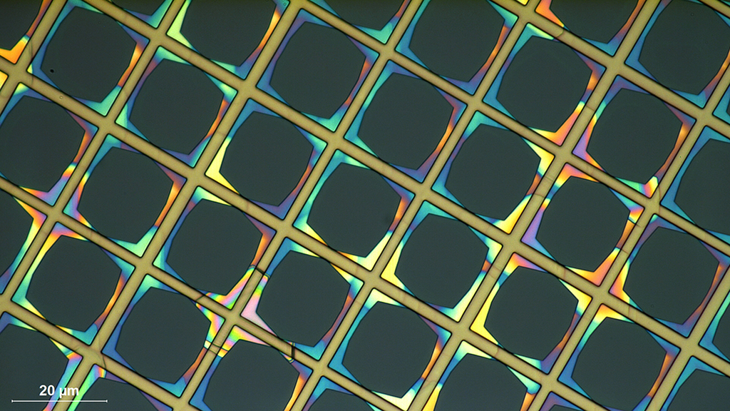
Contemporary microart
Remco van Erp, POWERLAB
Optical microscope picture of trenches in GaN on silicon with an undercut in specific crystal planes resulting in a picture that looks like it could be straight out of the museum of contemporary art. Maybe one day it will be worth a lot of money, but for now my best bet is the picture of the month. Made with Nikon Eclipse LV150.
