Back to the current year Winners
2020, December
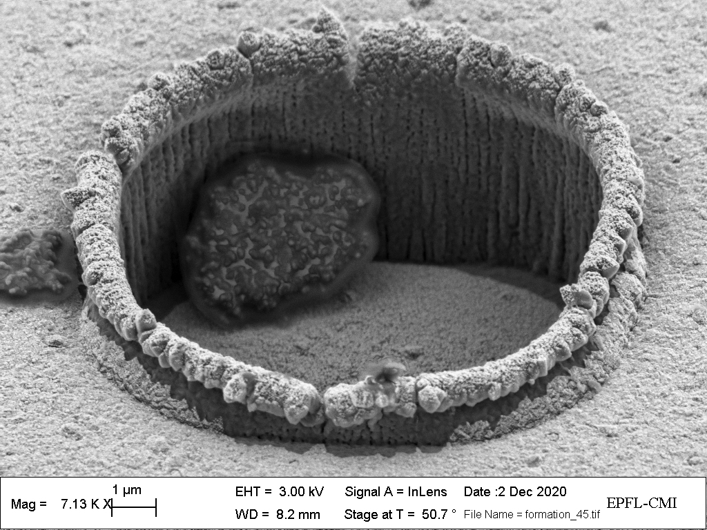
Survivor
Reuben Puddy, Oxford Ionics
The blob rests, exhausted but thankful to have survived the plasma storms that hit the gold wastelands of the night before. 15 minutes at high power in the Z02 Tepla Giga batch are enough to finish off even the hardiest of photoresists, but this little survivor found shelter in an unfilled VIA and lives to resist another day.
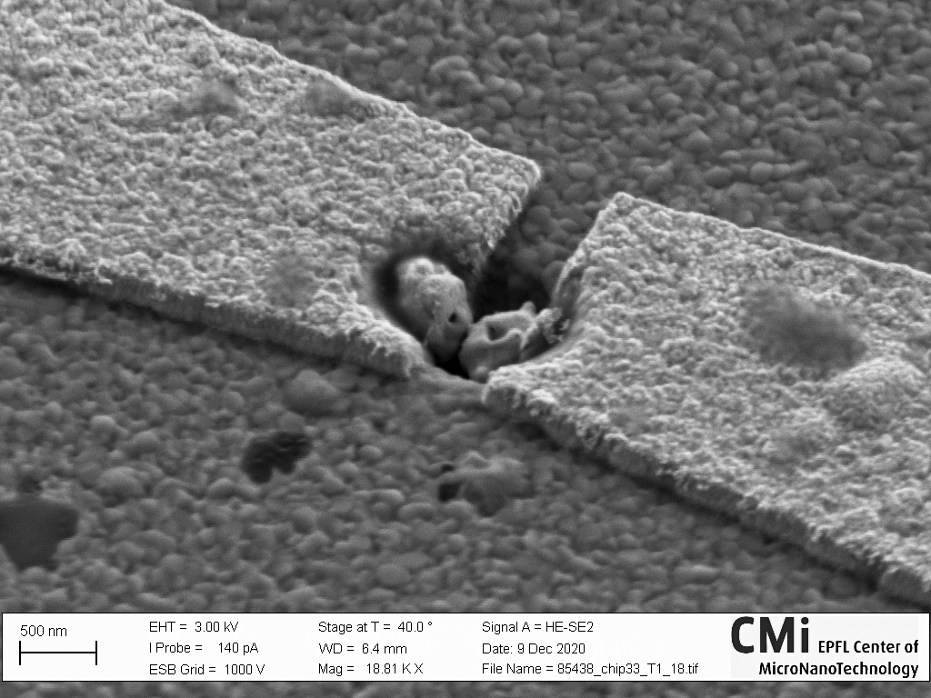
Nano kiss
Henry Shao-Chi Yu, LMIS1
Two Au nanoparticles are assembled and connected by electrodes respectively to form a pair of nanogap electrodes. Two AuNP are fused at the contact point, and it looks like a kiss between two nano-aliens.
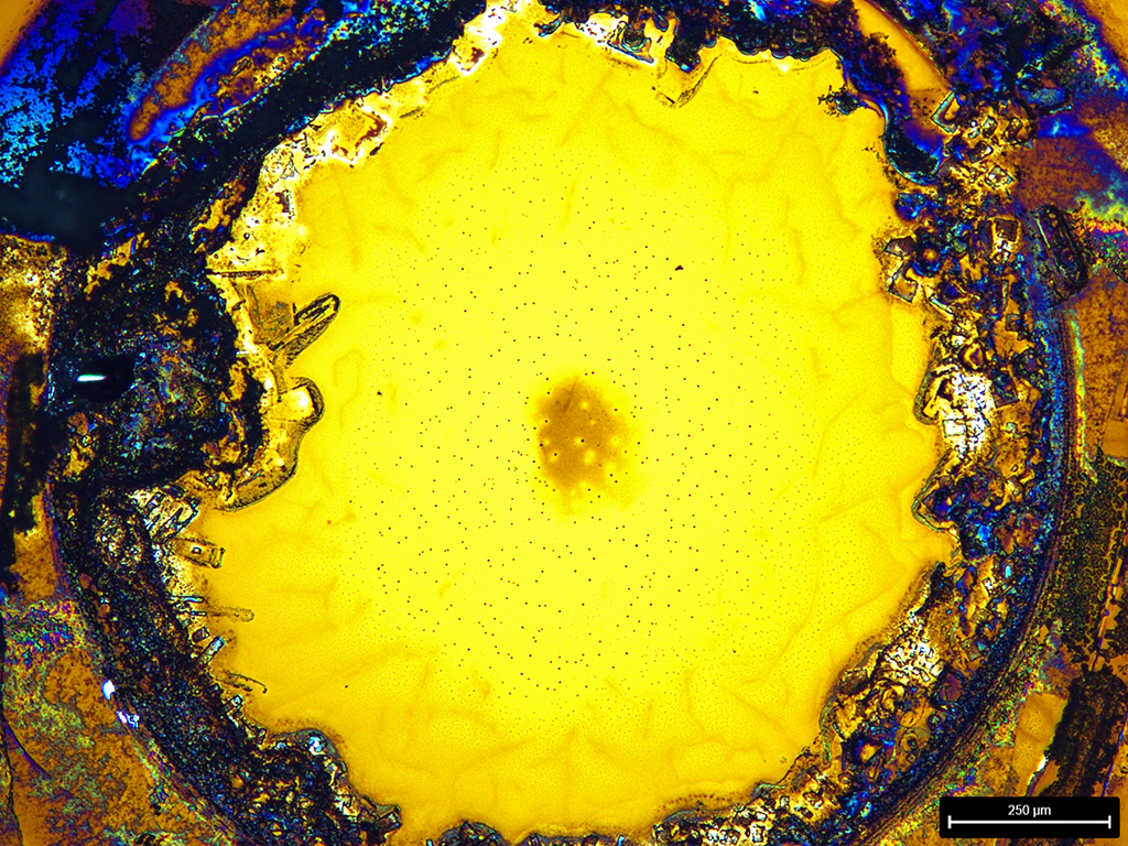
Eye see you
Stéphane Nilsson, INE
It is the defects that make us unique. The defect was found after making 50nm thick windows membrane for in-situ TEM observations. Its formation is still a mystery.
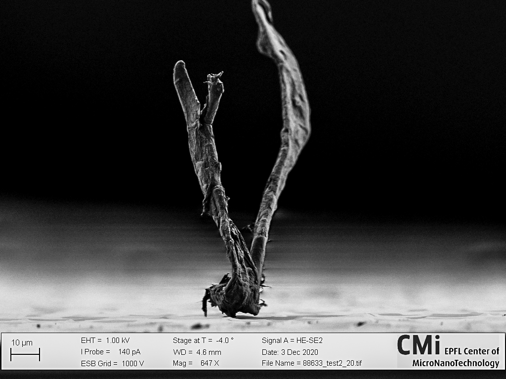
Desert rose
Henry Shao-Chi Yu, NanoLab
While taking images of a silicon chip cross-section, an unexpected object/defect was found on the wrong side of the chip, sitting there by itself, just like a dying desert rose. This reminds me of a song from Sting.
2020, November
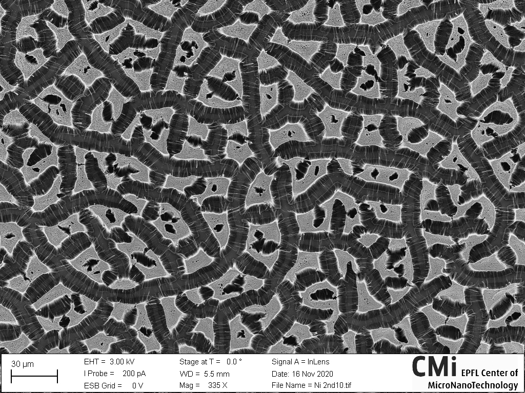
Nano Labyrinth
Pooya Dehghan, NanoLab
Can you find your way through this Labyrinth? Be careful, it is made of CNTs.
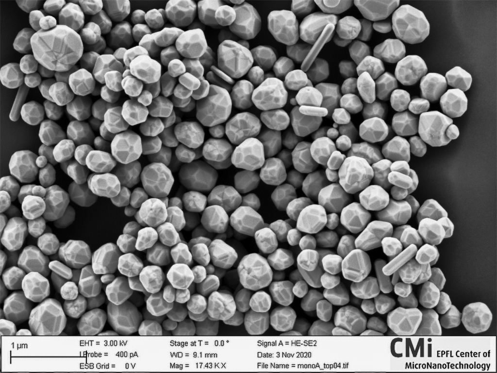
Gold mine
Marco Riccardi, Marc Bilger, NAM
One day, while looking for mysterious crystals on our silicon wafers, we stumbled upon this hidden gold mine! Gold nanocrystals, produced as a byproduct of a chemical reaction, agglomerated together thanks to Van der Waals interactions and landed on the substrate, ready to be picked up by any lucky nano-miner!
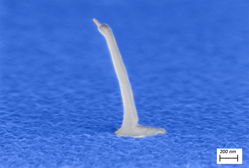
Swan lake
Shreyas Joglekar, Lucas Güniat, LMSC
In these cold greyish days, we reminisce in the fond memories of spending summer along the lakeside. Sunny sky, blue waters and swans swimming in lac Léman. This SEM micrographs shows a InAs-GaAs core shell nanowire on Si(110) substrate prepared in CMi. The processes include E-beam patterning and cleaning of the substrate. These were followed by Reactive Ion Etching (RIE) to form SiO2 nanopillars, on which the GaAs nanowires were grown using Ga droplet as a catalyst. The SEM image was captured in CIME. The nanowires were grown using Molecular Beam Epitaxy (MBE) using Ga droplet as a catalyst. The beak of the swan indicates unconsumed Gallium catalyst droplet.
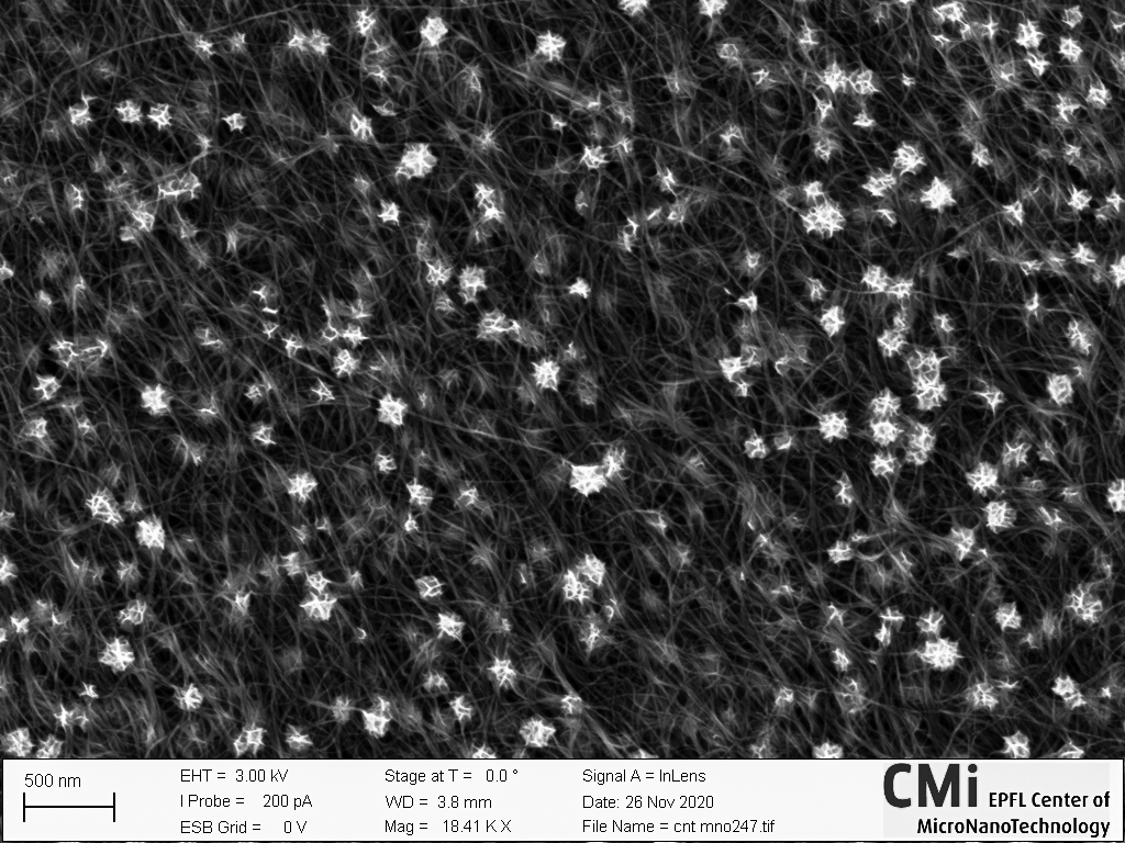
CMi Meadow
Pooya Dehghan, NanoLab
Enjoy the beautiful Nano flowers in the CMi meadow. But do not try to pick them! They are MnO2 nanoflakes grown on CNTs.
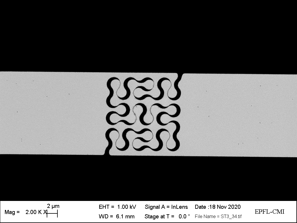
Membrane mismatch
Yi-Chiang Sun, LMIS1
The picture shows the released low-stress SiN membrane with a fractal design. The SiN membrane was patterned by DUV stepper, followed by a backside KOH etching to form a suspended membrane. The released membrane is deformed due to the release of the stresses.
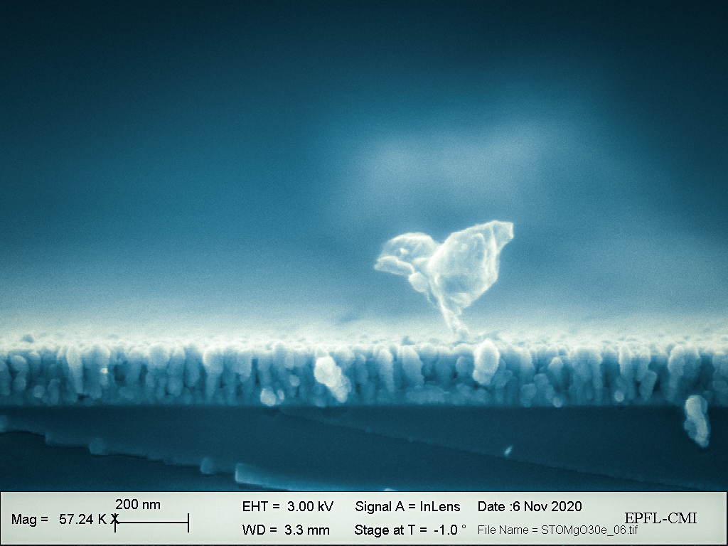
What sprouts in the ocean depth?
Wojciech Szmyt, EMPA
BaTiO3 film on MgO substrate, cleaved. Residues on the surface create curious shapes sometimes!
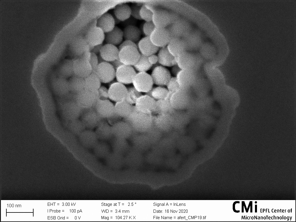
SiO pearls
Anna Varini, Q-Lab
White pearls of SiO sugar drop candies are tightly packed in the deep etched amorphous Si jar sealed with transparent film during CMP process. However, this particular jar is open, so go ahead and have a sweet treat.
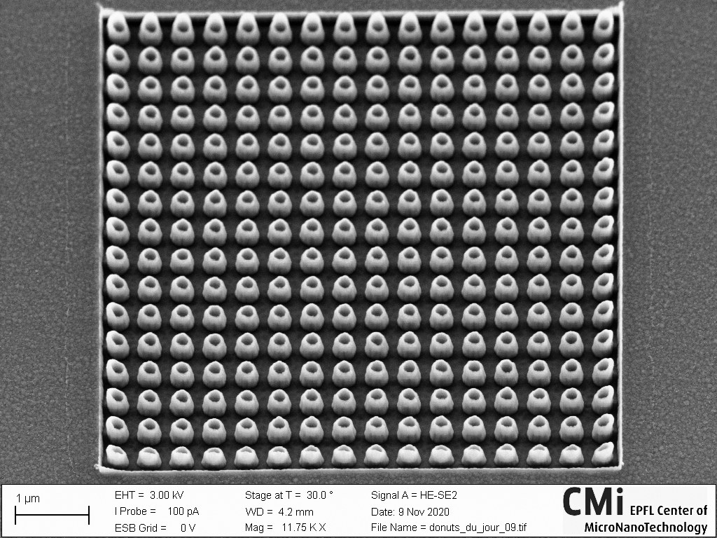
Donuts du jour
Anna Varini, Q-Lab
Another sweet specialty that looks like a full tray of muffins. Created by Ion beam Etching of amorphous Si. Original shape of the muffins is attributed to the Ion Beam Fencing effect.
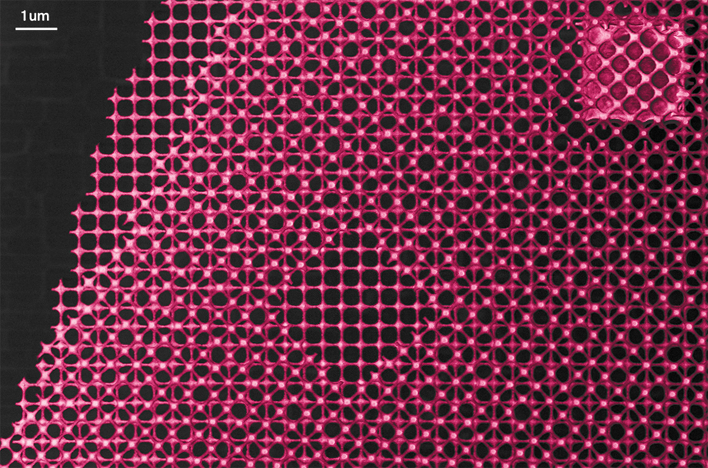
Knitted Silicon Nitride
Giulia Mongardi, NEMS
Lockdown in winter time? What about some knitting? This SiN membrane was obtained with DUV stepper exposure plus dry etching in TEL, AMS and wet etching in KOH. (Un)fortunately, it broke down creating this knitted-like pattern!
2020, October
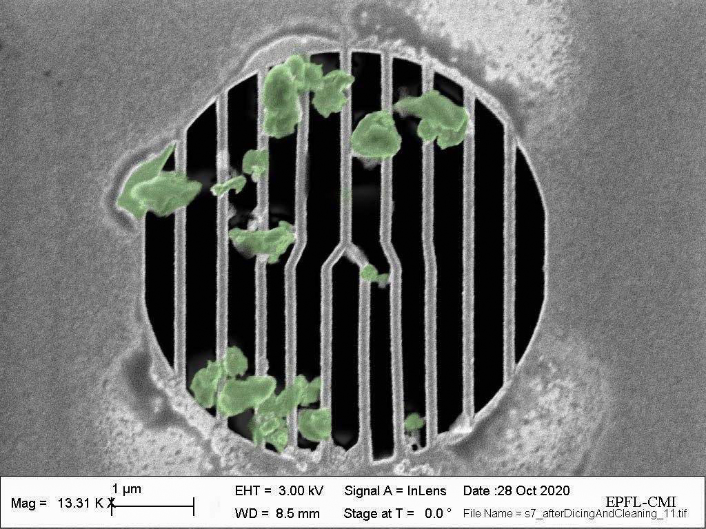
Escape from nano jail
Veronica Leccese, LUMES
Breaking news: ruthless nanoparticles just escaped from jail. Don’t go out of your home until further notice!
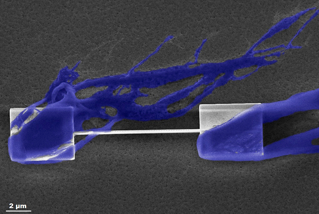
Spooky ghost of CMi
Pierre Lottigier, LASPE
Spooky things can happen if you don’t handle chips carefully… the ghost of CMi haunted my blue-emitting nanobeam lasers during Halloween! Do you think you can frighten him with Rapid Thermal Processing?
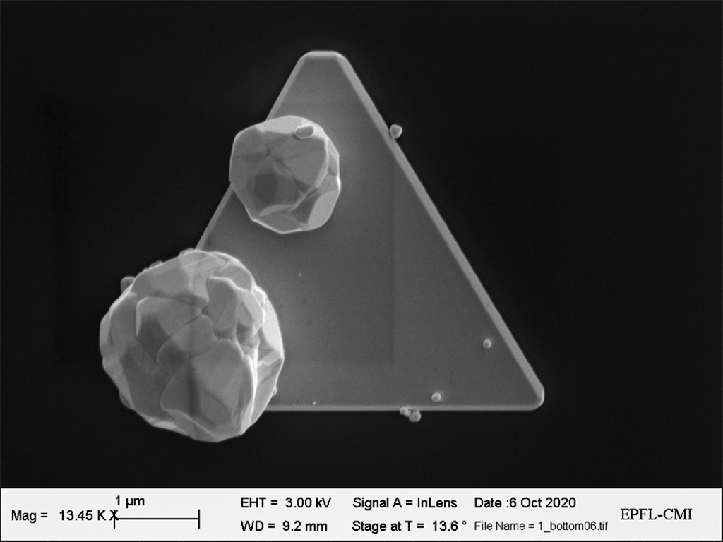
Crystallized beauty
Marco Riccardi, Marc Bilger, NAM
It’s easy to synthesize gold nanoparticles by reducing a gold salt in solution, but producing high aspect ratio monocrystalline flakes is much more challenging! Here you see a small and thin triangular flake grown on a silicon substrate, with two microparticles deposited on top. These are produced by uncontrolled coagulation of gold atoms, as opposed to the slow and controlled growth of the triangular crystal underneath.
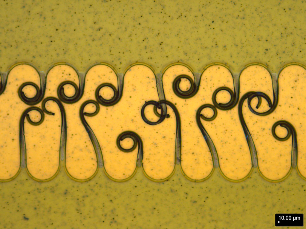
The tentacles of the sea
Eva Debette, GM-MA3
These Silicon flower buds, ready to bloom, were not farmed but etched with an excessive passivation. Etching eventually made its way vertically down to reach some buried SiO2, and to slightly notch the stalks for the flowers now ready for pick-up.
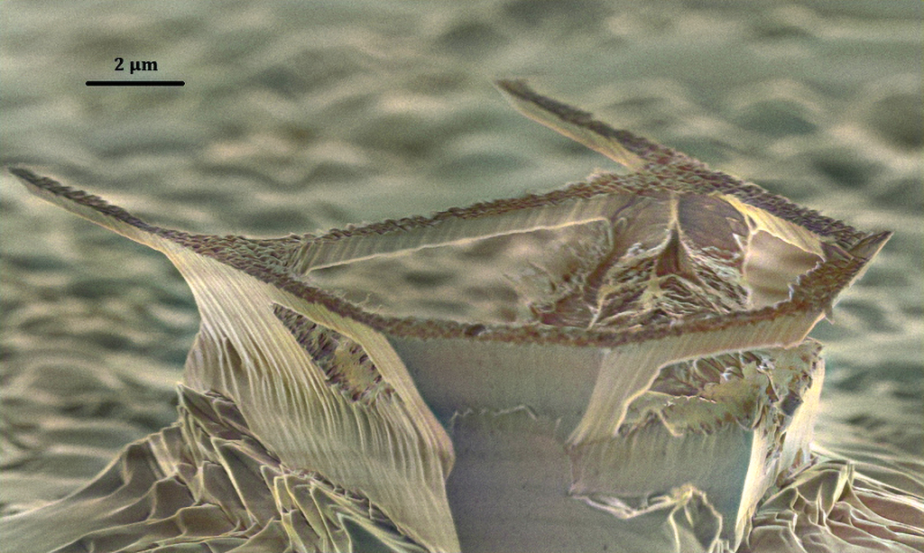
Starship “A”nterprise
Sichen Mi, Q-lab
After a disastrous oxygen plasma storm, our starship landed on the single crystal diamond planet. The structure was carved in a bulky diamond substrate. To achieve this – a cone-shaped Faraday cage was fed to STS main chamber to perform undercut from all directions. For some not yet identified reason the etching was a complete chaos, but the marker “A” happily started serving the Starfleet.
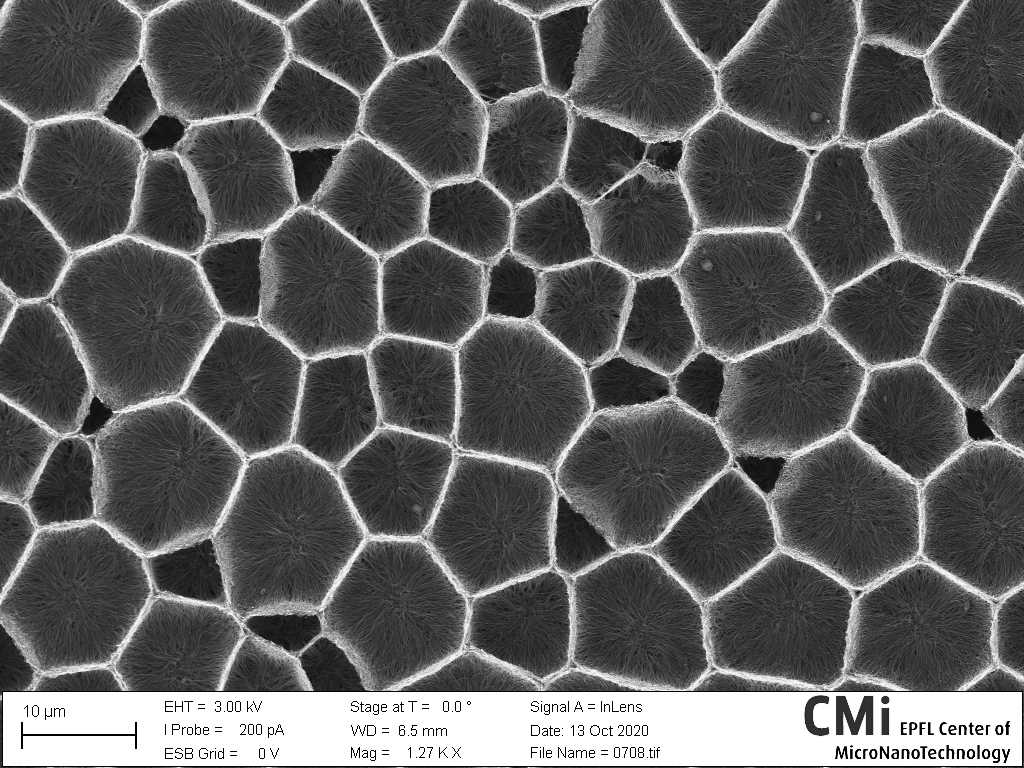
Micro CMi wasp nest
Pooya Dehghan, NanoLab
Don’t expect honey inside them, because they are made up of CNTs!!!
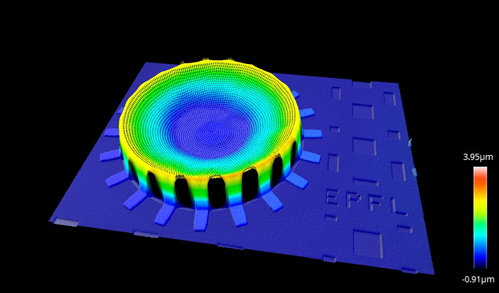
EPFL’s micro Colosseum
Amir Youssefi, LPQM
Exploring in CMI we discovered an ancient stadium. A superconducting vacuum-gap capacitor.
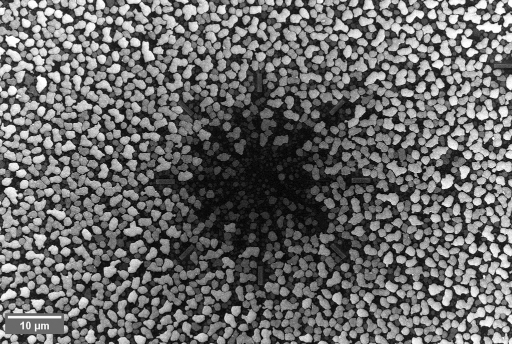
Halloween Blackhole
Elif Nur Dayi, LMSC
Marshmallow like oxide particles are being tucked away by our nanowire array of GeSn alloy, which clearly feels the Halloween spirit with its spooky look.
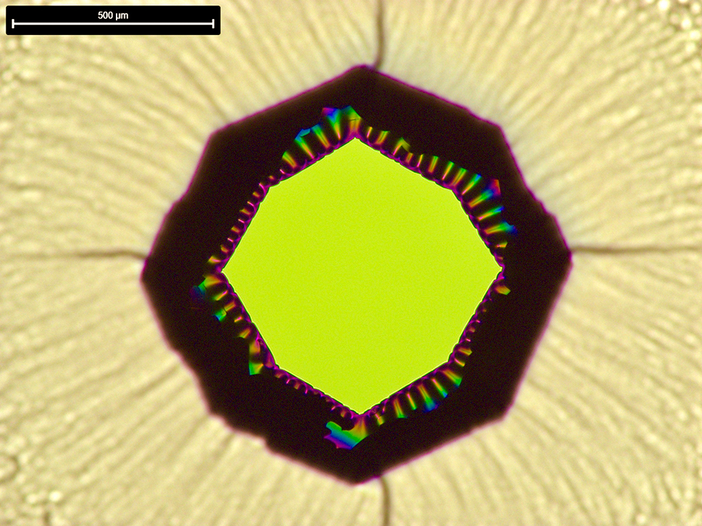
KOH dot focus
David Di Stadio, LMIS1
Picture was taken after the KOH etching with the SiO2 mask still on. We can see the whole structure with the same interference pattern from the SiO2 mash and a organic-like background which is only the bottom surface of the Si after KOH etching.
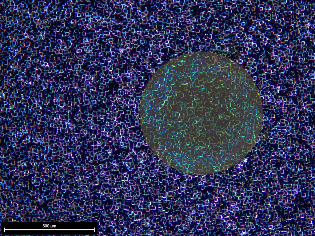
Dark Side of the Moon
Sylvain El-Khoury, CERN / EP-URD
As it’s getting dark sooner and sooner lately, we get many opportunities to observe the sky, while leaving the lab in the evening. Out of this this ocean of stars, the Moon may attract your attention for being full and bright for the second time this month! Could our satellite be the inspiration of this 500nm SiO2 membrane, shining on the backside of its Si wafer?
2020, September
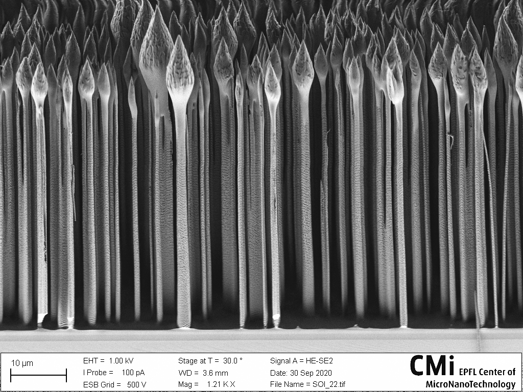
Silicon Flower Buds
Joffrey Pernollet, CMi
These Silicon flower buds, ready to bloom, were not farmed but etched with an excessive passivation. Etching eventually made its way vertically down to reach some buried SiO2, and to slightly notch the stalks for the flowers now ready for pick-up.
2020, August
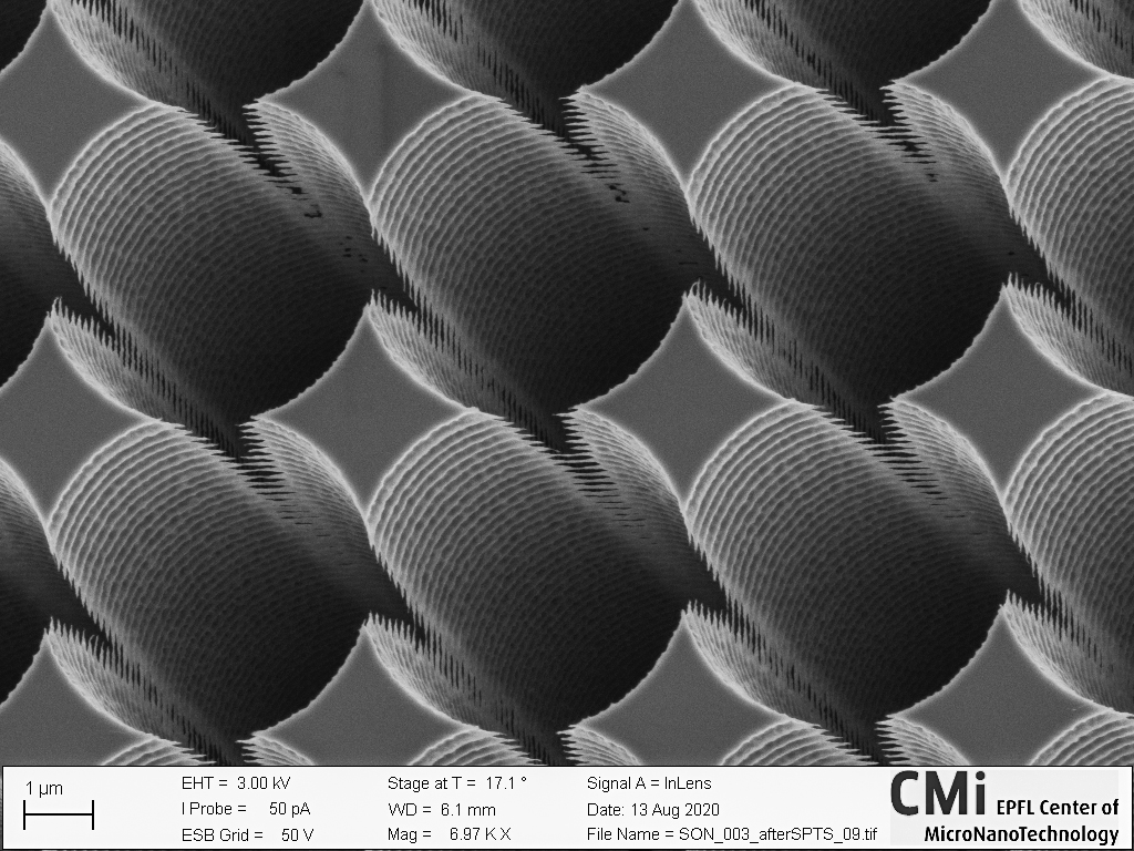
Groovy !!!
Clémentine Lipp, LMIS4
Assume the distance between neighboring circles is smaller than the under-etch of a standard Bosch process, etch and let it groove!
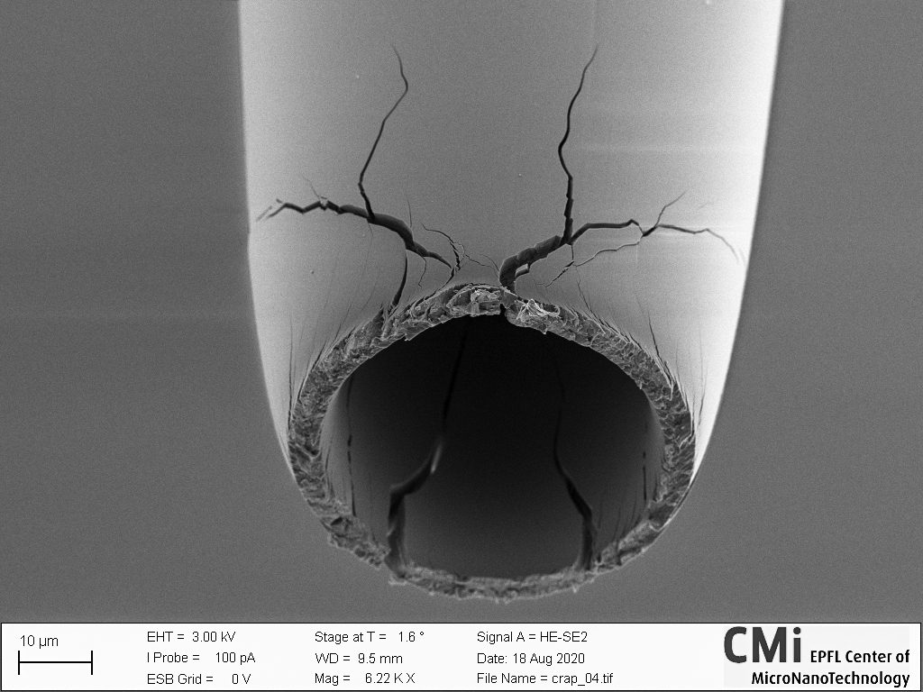
Pain
Simon Finn Mayer, LBM & LBEN
Glass capillary realizing that life is pain. Side view of a physically and mentally broken glass capillary imaged in CMi’s Zeiss MERLIN SEM.
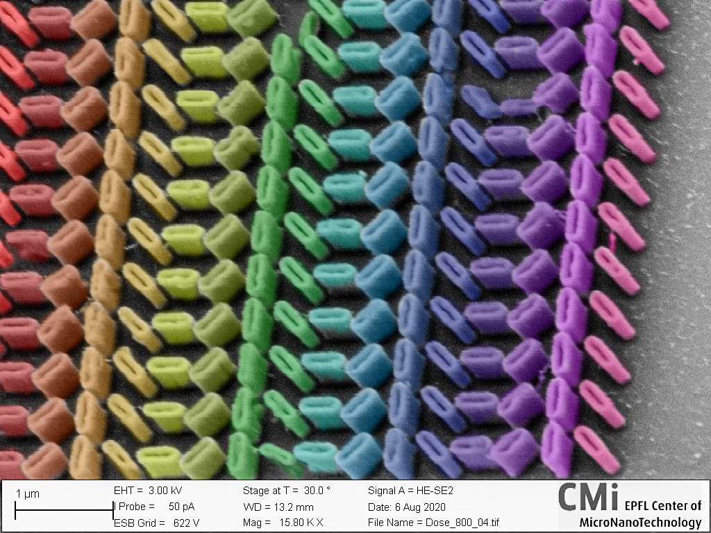
LGBT’s of the nanoworld
Debdatta Ray, Cervinka Ondrej, NAM
To support the LGBT’s of the nano-world, we made TiO2 meatsurface whose features come to display the rainbow flag.
2020, July
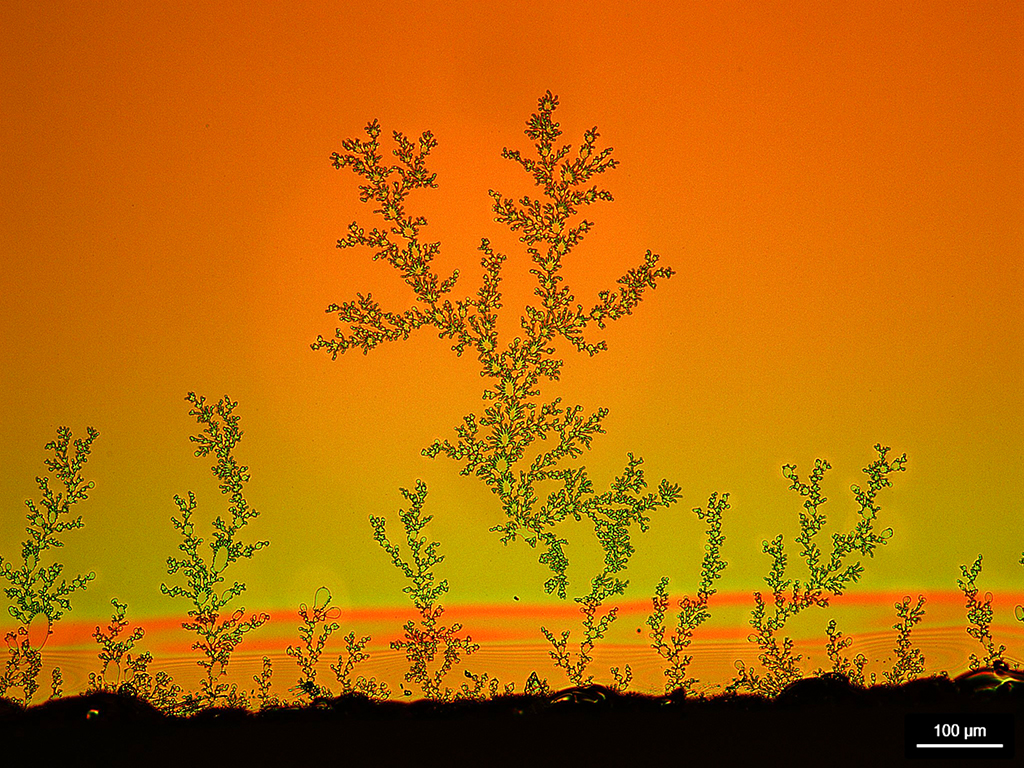
Sunrise
Nicolas Maïno, LMIS4
As sun rises, light reveals a forest of elegant trees on this wafer horizon. The trees are formed from salt residues that dried up in a fractal fashion after photoresist development while the thin oxide layer gives this image its warm glow.
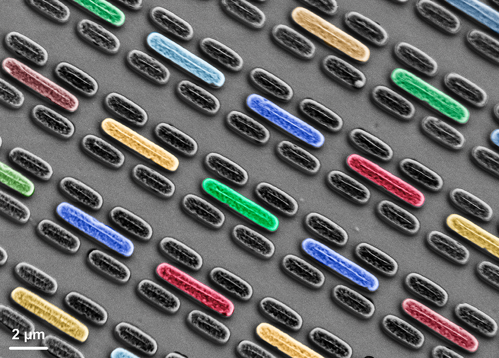
Plasmonic race cars
Aleksandrs Leitis, Ming-Lun Tseng, Deepthy Kavungal, Aurelian John-Herpin, BIOS
The work in academia is vibrant, stimulating and overall very exciting. Yet, it comes with the cost of potentially lower salaries than elsewhere. Therefore we cannot afford luxurious F1 sports cars. Luckily, with the deep UV lithography processes at the CMI we can fabricate millions of “Ferraris” and “McLarens” in the time scale of seconds. Here we present durable aluminum-based plasmonic F1 race cars at slightly smaller scale than their real life counterparts… Strikingly, they are not only amusing, but also highly practical for label-free biosensing applications.
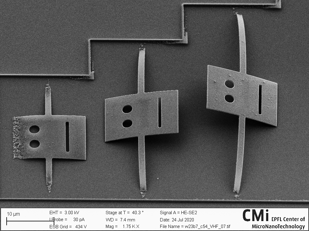
Stressed micro-people
Micol Previde Massara, Hamed Sattari, Q-LAB
We were studying stress-induced buckling in poly-silicon beams after release, when we noticed that our micro-citizens are very scared of vapor HF attack. The “stress” caused all of them to break, two of them to completely lose their hair, and the one in the front to sweat out of fear as well!
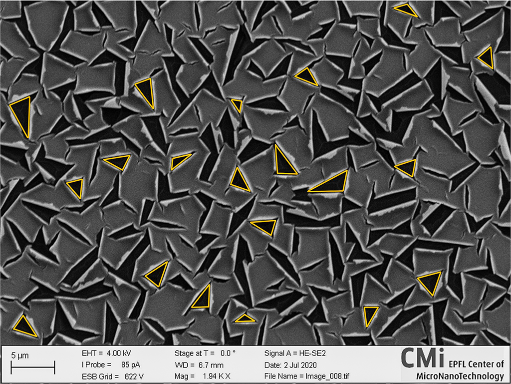
Illuminati confirmed
Debdatta Ray, Cervinka Ondrej, NAM
The secret message hidden in a chromium coating over PMMA can only mean one single thing: “Illuminati confirmed!”
2020, June
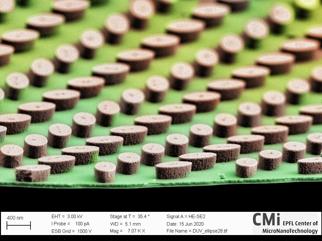
Tiny tree stumps
Aleksandrs Leitis, Ming-Lun Tseng, Deepthy Kavungal, BIOS
Once again the lumberjack has visited the Merlin SEM leaving behind these nicely cut tree stumps. Interestingly, the tiny timber does not only create lucrative business, but also has exciting optical properties. The specific cut of the tree trunks allow to achieve high surface sensitivity for biomolecule detection. On top of that, these stumps are ideally suited for integration in point-of-care biochemical sensor devices.

A cheesy affair
Matthias Neuenschwander, LBNI
Eating is obviously forbidden at CMi, but someone managed to get slices of Parmesan cheese onto my wafer! Did they hold a late night pasta party in zone 15? I suspect we will never know. A silicon dioxide mask was under-etched in KOH. The mask collapsed after the wafer was dried. The holes in the oxide give it a distinctly cheesy look.
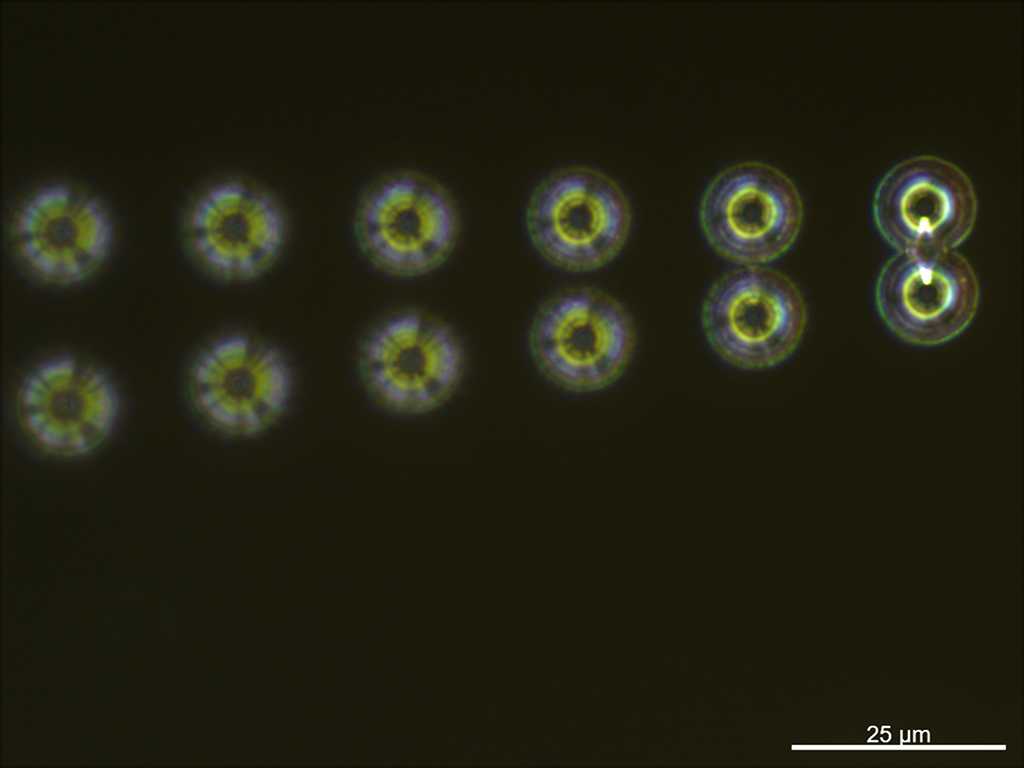
Shining encounter
Clémentine Lipp, LMIS4
Underetch of small holes walking towards each other gives rise to this beautiful optical effect.
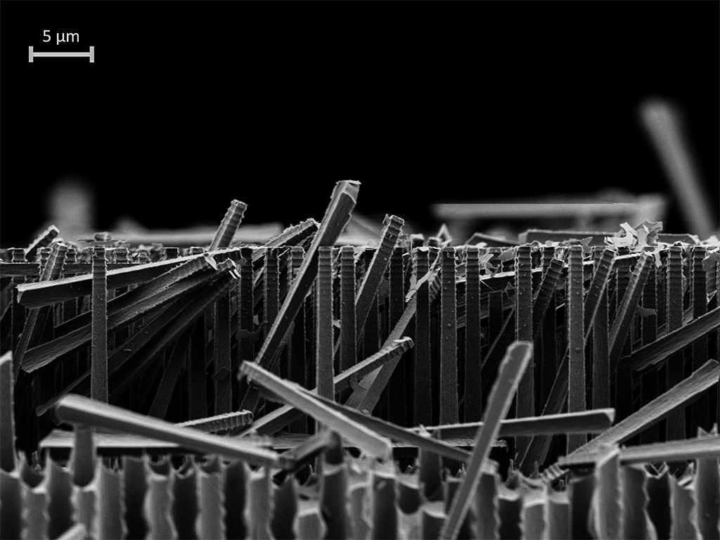
Playtime at CMi
Samira Frey, PVLAB
For the fabrication of amorphous silicon based microchannelplates we are currently optimizing the deep reactive-ion etching with a metal mask. During the first tests some of the structures collapsed due to too much under-etching, leaving us with what looks like a game of Mikado.
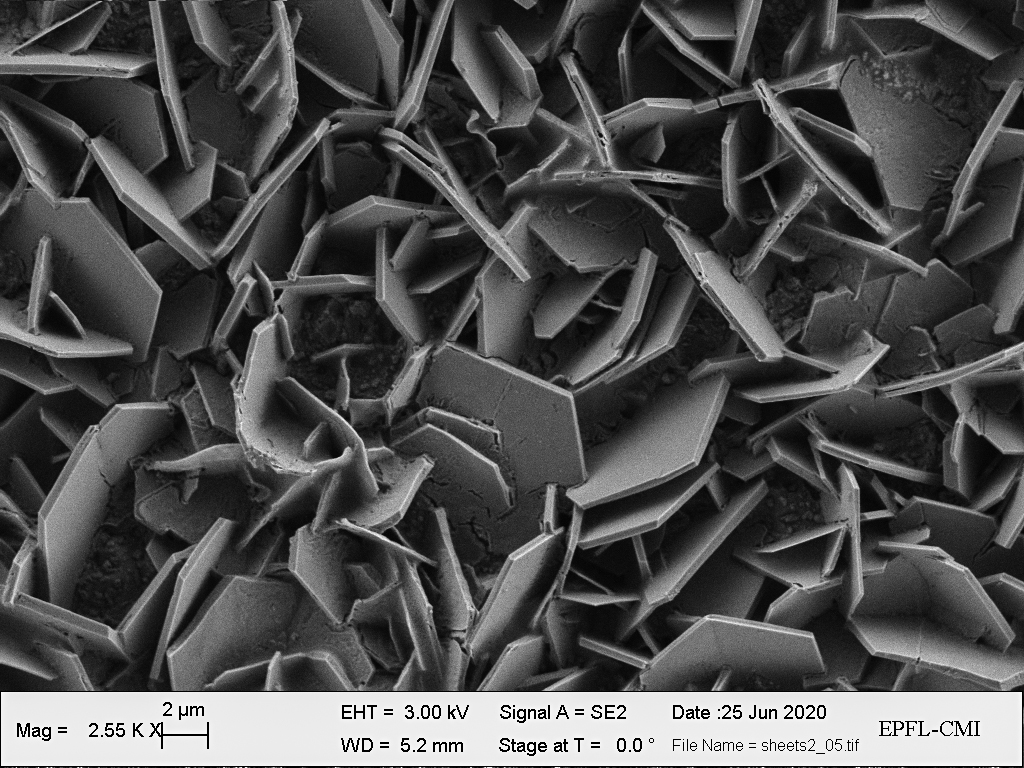
Sheets
Pooya Dehghan, NANOLAB
MnO2 crystals deposited on the substrate from a Manganese acetate solution using electrodeposition technique.

Broken blue bridge
Pierre Lottigier, LASPE
“We build too many walls and not enough bridges” did Sir Isaac Newton anticipate that hundreds of these bridge-like nanobeam structures could be built within hours? The problem is that some of them get broken and nobody cares… How would you repair this one? III-N blue emitting nanobeams, <300 nm thick membrane.
2020, May
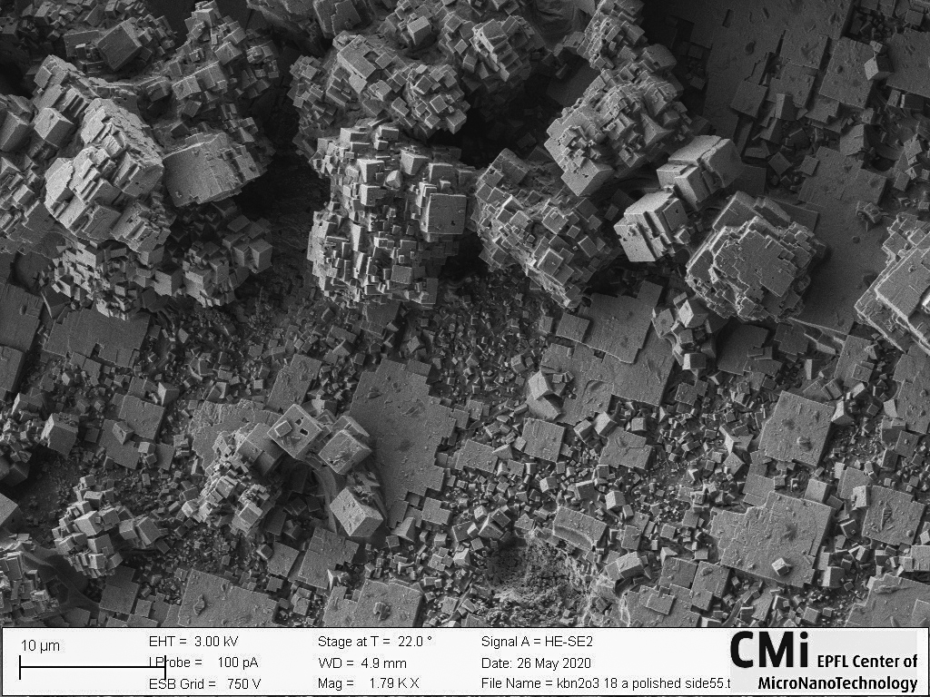
Ruins of an ancient Celtic city
Luka Ćirić, LPMC
In the image one can see the cubes of KNbO3 crystals grown on SrTiO3 substrates.
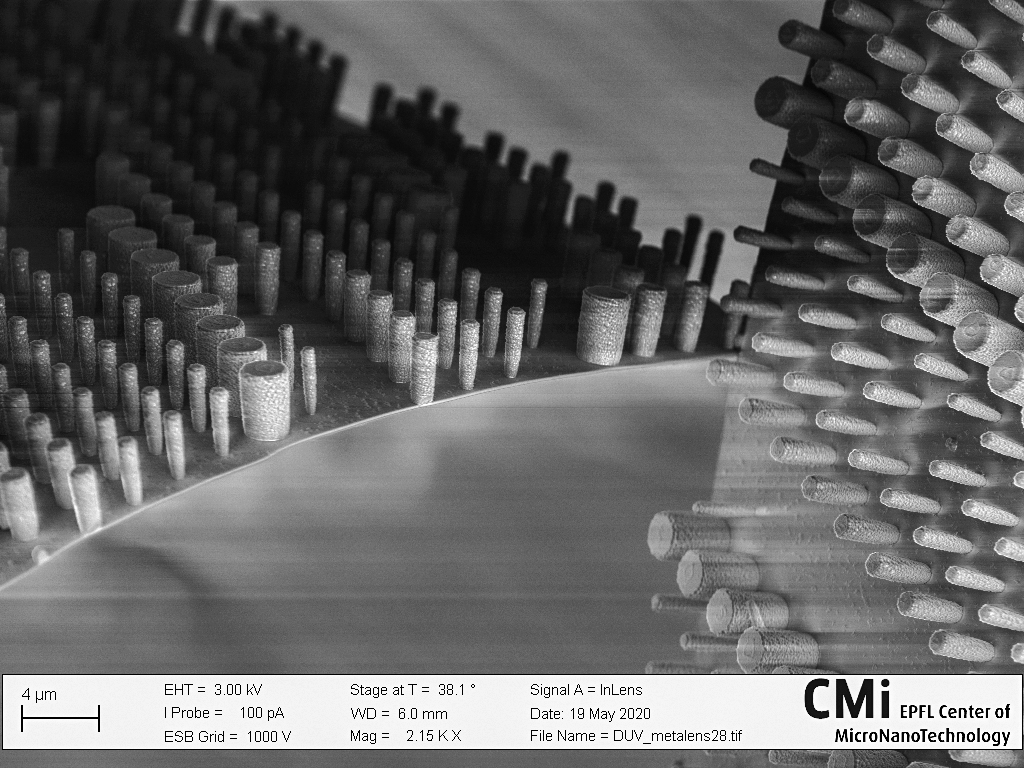
Inception in SEM
Aleksandrs Leitis, Ming-Lun Tseng, BIOS
We have always dreamed of controlling the metasurface physical properties at will. By incepting the SEM, we have moved one step closed to this dream. You can see the results which were acquired with the powerful Merlin SEM in the image above. These ultra-thin metasurfaces were meant for light wavefront control and highly efficient light focusing.

Sunflower metalens
Aleksandrs Leitis, Ming-Lun Tseng, BIOS
While being in remote and rural places during the lockdown period, the BIOS lab members were inspired by the nature itself. Specifically, by sunflowers, which triggered us to fabricate metalenses with particular pattern that allow us to gather IR light with high efficiency.
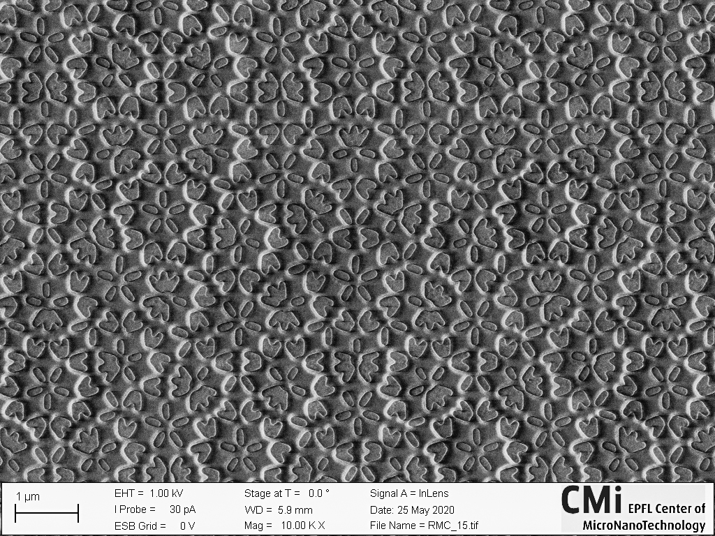
Quasicrystalline “Hanami” flower
Sho Watanabe, LMGN
Do you know the Japanese traditional custom called “Hanami”? In spring, we Japanese gather together near cherry trees to enjoy their beautiful flowers, sharing some alcoholic beverages as well. Unfortunately, during the lockdown of Switzerland we needed to refrain from Hanami this year. Still, thanks to the re-opening of CMi, cherry blossom-like quasicrystalline flowers (based on Penrose P3 tiling, exhibiting five-fold rotational symmetry) made out of NiFe have been successfully fabricated via lift-off processing. As these nanostructures were cleaned with acetone and IPA, one of the important parts of Hanami, enjoying alcohol, was accomplished! And by admiring these “flowers”, you step into the Japanese culture and complete the tradition!
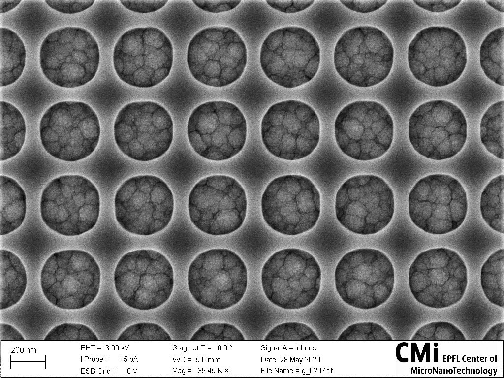
Swiss Cheese on a Whole Wheat Bread
Dorian Herle, Q-LAB
This healthy snack was created in the CMi cleanrooms using e-beam lithography. It shows a patterned ZEP resist on a sputtered amorphous silicon layer. Its textured surface is clearly disguisable from the smooth ZEP surface.
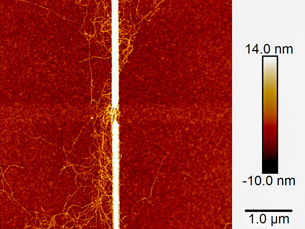
NanoSparks
Pierrick Clément, LMIS1
The AFM picture shows the immobilization of single-walled carbon nanotubes (SWCNTs) between a pair of platinum electrodes on silicon substrate by dielectrophoresis. The assembly of the SWCNTs follows the applied electric field and looks very similar to electric sparks (but at the nanoscale) when an abrupt electrical discharge occurs creating a conductive channel through a normally insulating medium. This picture is dedicated to the bright sparks of the CMi! The image was recorded in CMi (Zone 15) on Bruker FastScan equipment. The device was fabricated by E-beam lithography and photolithography at the CMi.
2020, April
Chrome mask
Georges-André Racine, CMi
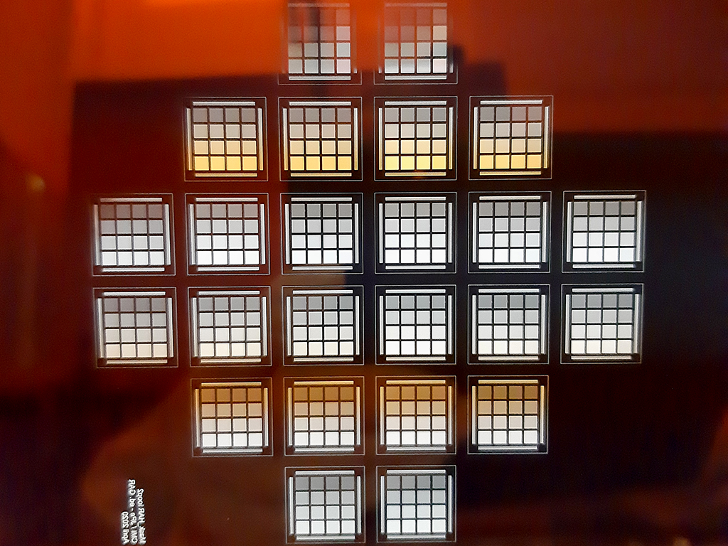
This picture shows colored windows in a white light transmission mode through a Cr-mask. This particular test mask for the evaluation of a high aspect ratio etch tool was the first one fabricated after the COVID-19 shutdown in the last days of April to verify functionality of the photolithographic equipment after its re-start.
Laser writer test
Georges-André Racine, CMi
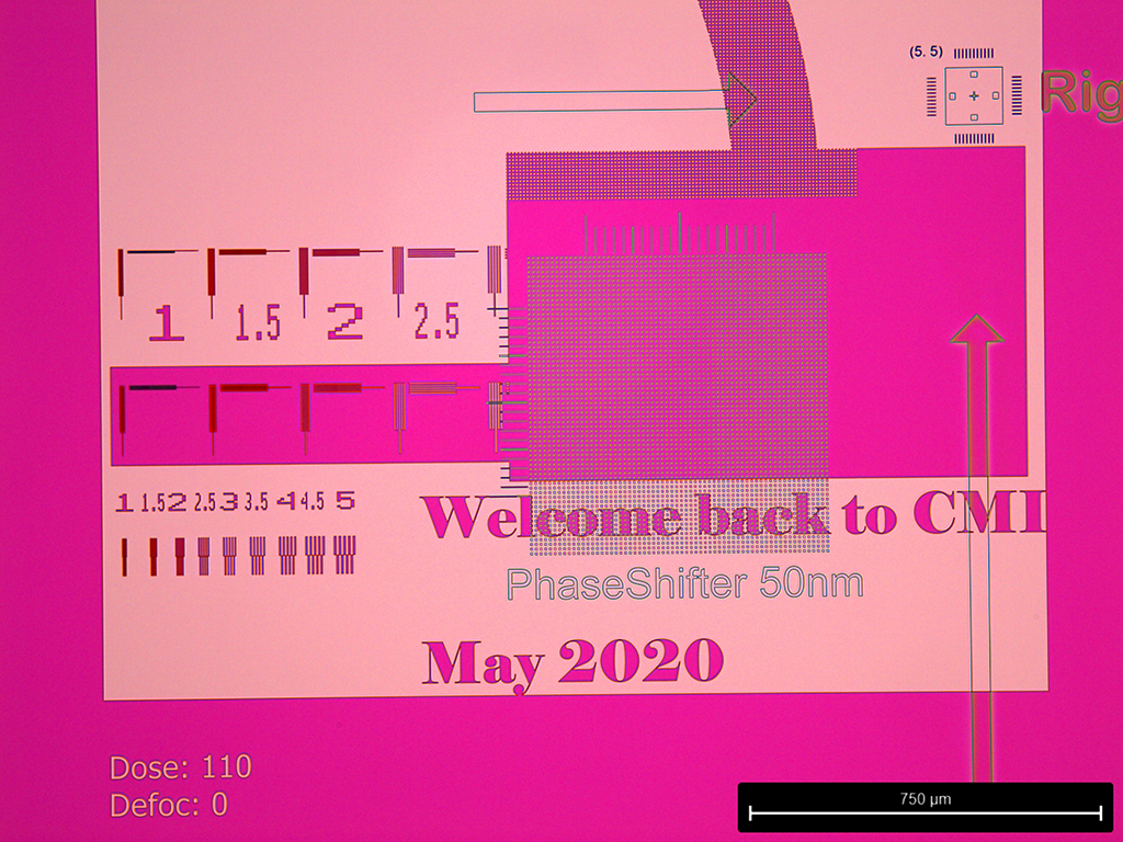
Various test structures written by direct laser writing into resist to verify its performance after the CMi re-start in the last days of April.
2020, March
Fishing boat at the gate of a canal
Gözden Torun, Galatea Lab
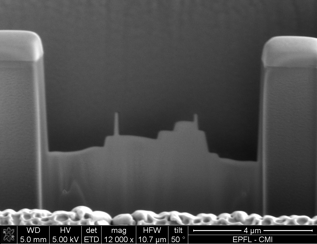
March, the month when the nature starts to wake up, has finally arrived. I am daydreaming of a boat trip with my family along the Mediterranean coast of my country. Suddenly, my daydream becomes a true picture on my ternary tellurite glass during TEM lamella preparation. The ternary tellurite glass which is quite sensitive to heat started to melt during lamella thinning in the FIB. Image was taken in FEI Nova 600, and sample is tilted 52°. The boat actuates with the electron beam, as boat in the rough sea.

Nanopillar Sunset
Lucas Güniat, LMSC
Here we are, just you and me, admiring this beautiful sunset over the sea of Si nanopillars. This optical microscope scene was taken at the corner of a 200nm-diameter Si nanopillars array manufactured by reactive ion etching. Spin-coating a fine layer of polymer creates light interferences at the corner of the array, giving this bright intense orange color. The stars in the sky are nothing more than impurities in the polymer layer. It’s getting dark now… are we gonna start the campfire?
2020, February
The Kubrick Crystal
Didem Dede, LMSC
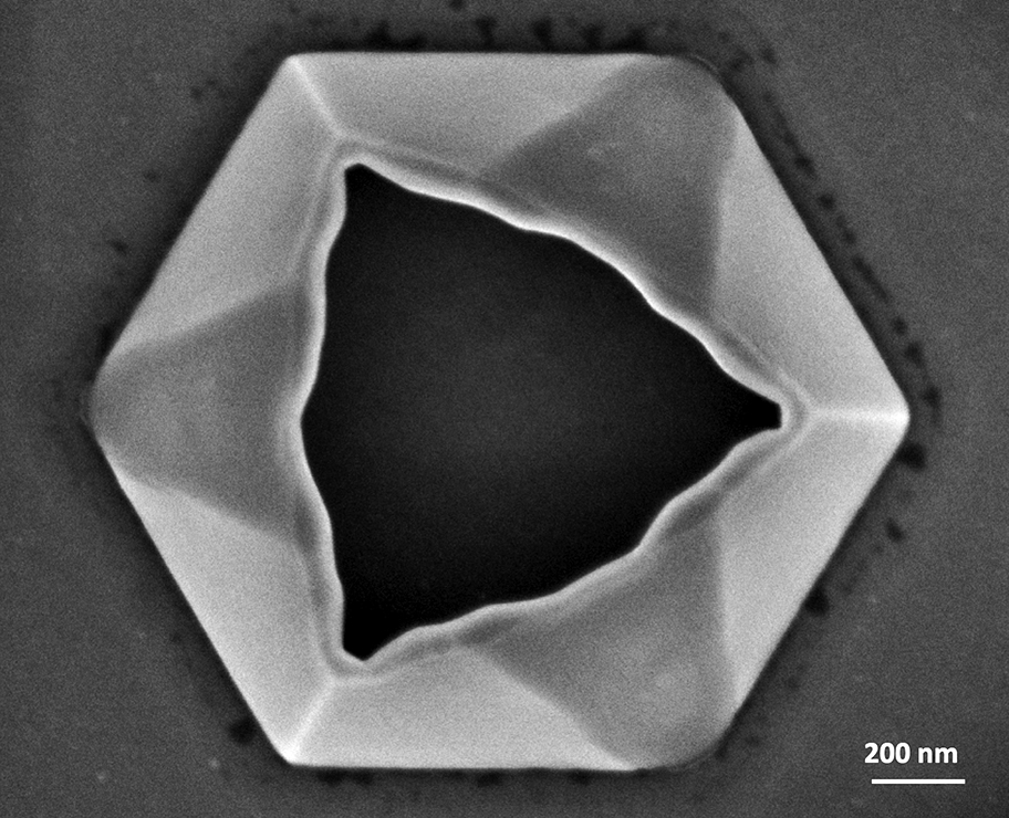
Symmetry has always been the basis of beauty. In this image, you see the selective area epitaxial growth of InAs/GaAs crystal. Due to the growth environment, we observe this overgrown structure.

Mirror, mirror
Clémentine Lipp, LMIS4
Mirror, mirror on the wall, who’s the fairest of them all?
Platinum walls
Sadegh Kamaei Bahmaei, NANOLAB
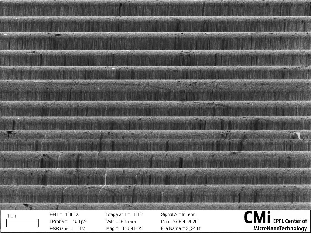
Monolayer of graphene on top of the platinum electrode at a slow SEM image scan. Even the micro-world is scared of Corona and it tries to build a lot of walls to protect itself from the virus.
2020, January
Modern Architecture Micro-Dome
Amir Youssefi, LPQM
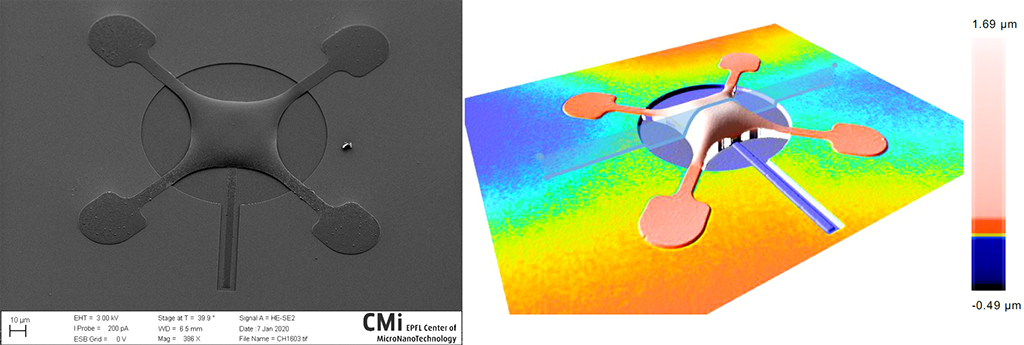
This suspended micro-dome is actually a high-Q trampoline mechanically compliant superconducting parallel plate capacitor used in quantum electro-mechanical systems.
Nano-foldable Keyboard
Hamed Sattari, Alain Yuji Takabayashi, Q-LAB
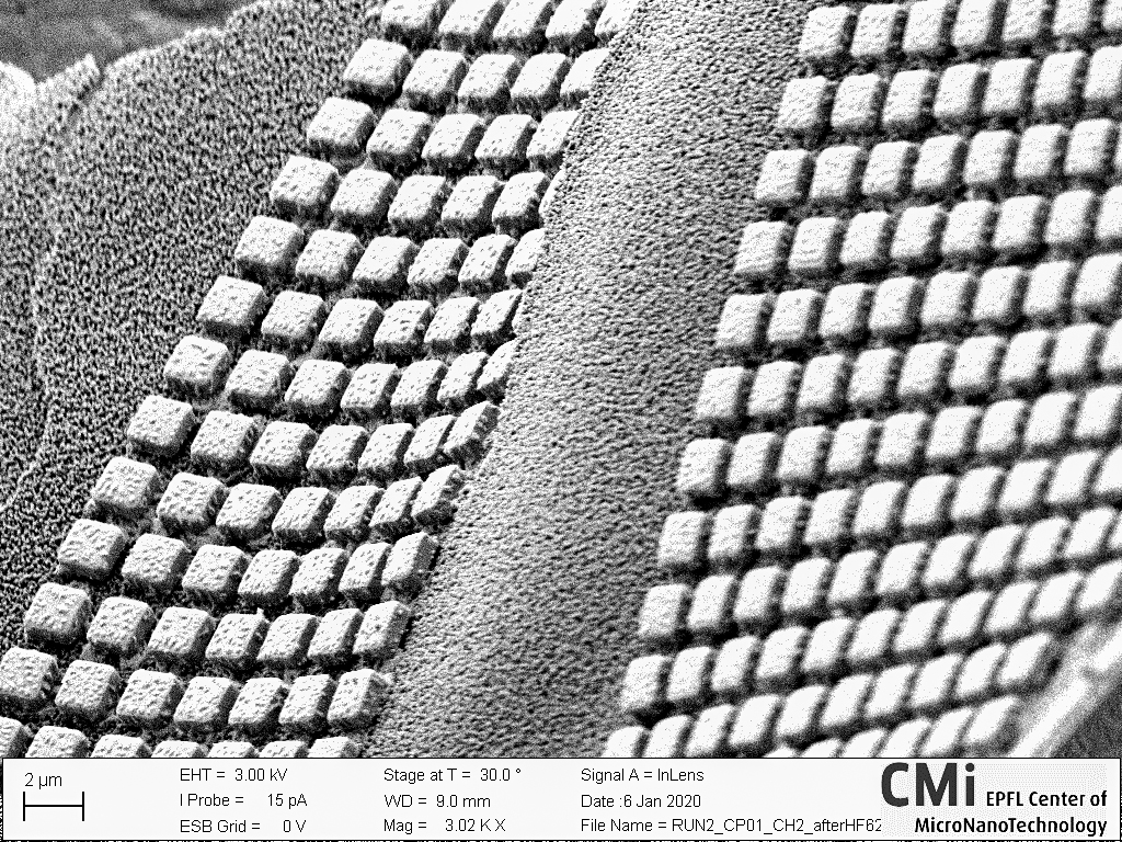
We passivate our photonic chips by an alumina layer deposition to protect the stack from HF vapor attack. Here, the passivation was not perfect, and consequently, the HF attack peeled of a filler structure layer, which looks like a foldable keyboard.
Starry Nano-light
Ming Lun Tseng, BIOS
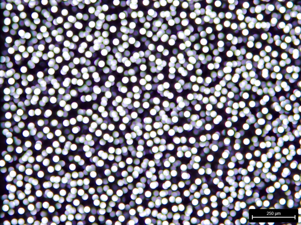
From GNN’s Ming Lun Tseng in Lausanne: The long-lost, Vincent van Gogh’s last painting “Starry Nano-Light” is finally found, in the CMi clean room, EPFL, Lausanne. It is believed that an anonymous collector hided it in this world-class facility to prevent its damage from brutal people during the lab cleanup activity. Different from Vincent van Gogh’s other works, this painting was made by performing reactive ion etching on a 380-um thick, high quality double side polished, 4 inch silicon wafers for 1 hour 4 minute 30 seconds to create a nanostructure on the top, which scatters light into the sky. Now this art work will be sent to Landesmuseum for a further evaluation of its value.
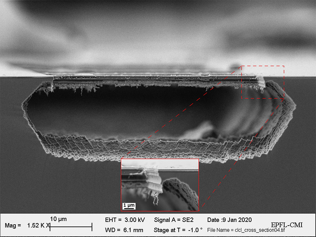
Sinister cave
Kaitlin Howell, Marco Liffredo, Jialiang Fan, NEMS
While searching with Indiana Jones for the Sankara stones, we stumbled upon a sinister cave, full of traps and unlucky trespassers. Stalagmites and stalactites made venturing inside dangerous. The cave was creating during the release of Si3N4 beams with AlN/Pt electrodes through Bosch and isotropic Si etching, which left residues on the surfaces. Further KOH etching produced the pyramid structures along the bottom of the cave.
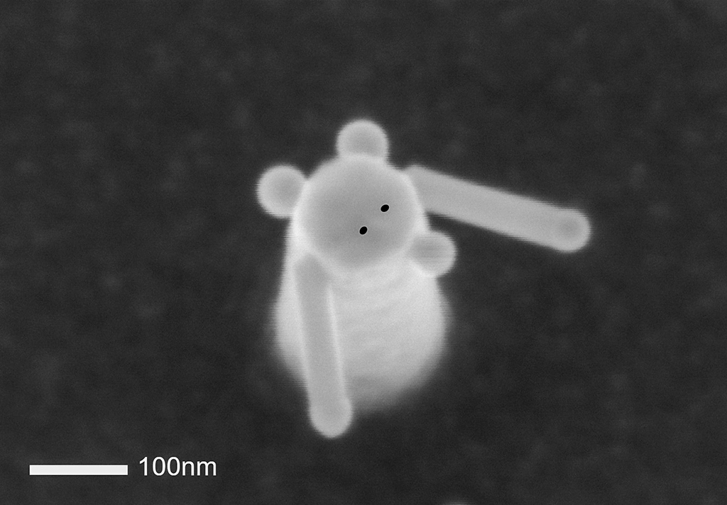
Cmouse
Lucas Güniat, LMSC
You guys should really be more careful while cleaning! I even found a Si nanopillar mouse on my chip! And on top of that with GaAs nanowire arms grown by Molecular Beam Epitaxy! Am I authorized to borrow the Nano-cat from Clementine Lipp (see June 2017 images below) to hunt it?
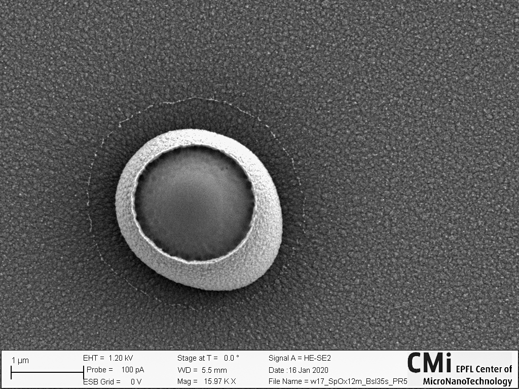
μVolcano
Micol Previde Massara, Q-LAB
After oxide sputtering and etching, micro-volcano structures formed on the wafer.
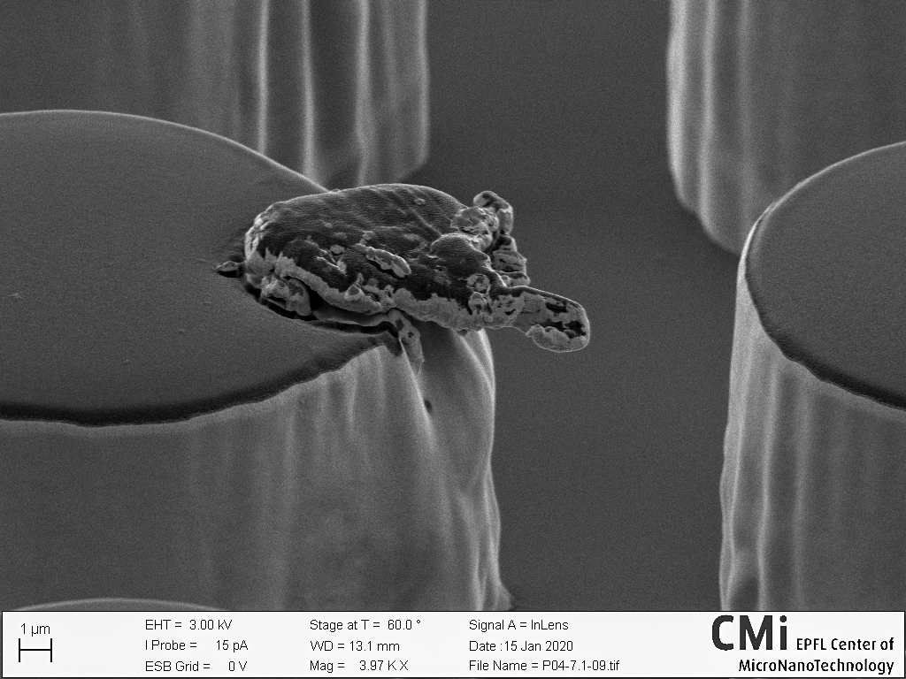
Turtle diving into ocean
Kevin Keim, Gloria Porro, CLSE
In January 2020 this titanium-platinum turtle is diving from the sharp edge of a new teardrop-shaped 3D electrode into the ocean, discovering new shores. “Bye, bye CMi. Thanks for the great time. I will send you a postcard.”
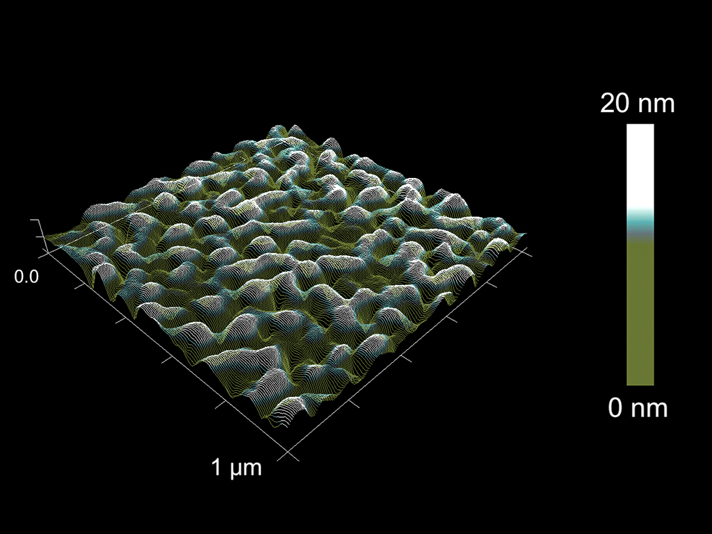
Germanium hills and valleys
Nicolas Humblot, LMSC
The recent snowfalls have evenly covered the mountain tops in Germanium ski resort. The snow/rain limit is worryingly rising as temperature does. Germanium film was grown by sputtering on top of a Silicon substrate. The image was obtained with AFM in Z15, FastScanA tip, ScanAsyst in Air mode.