Back to the current year Winners
2016, December
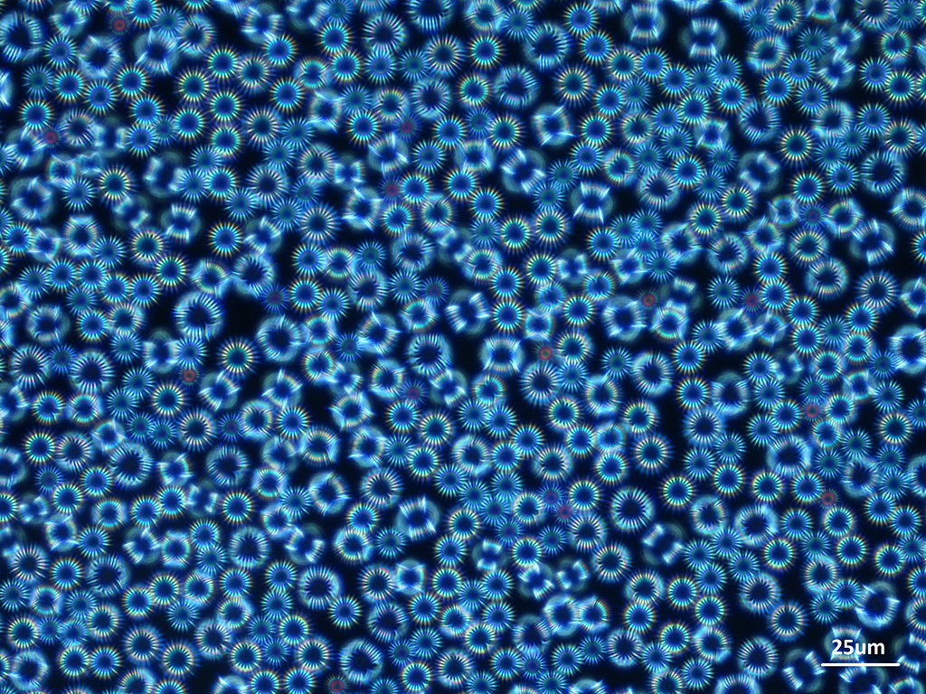
Starry night
Benoît Desbiolles, Clarisse Vaillier LMIS4
Valentin Flauraud, LMIS1
When you put cells on 3D nanovolcanoes, you start to sight heaven… Human Embryonic Kidney (HEK) cells cultured for 3 days on 3D nanovolcanoes were observed using optical microscope. By playing with the focus, we could transform the water droplets covering the sealing into stars. 80%CMi, 20%LMIS4.
2016, November
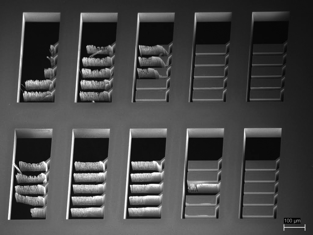
Silicon Valley after an earthquake
Miloš Hrabovský, Tescan
Xenon plasma Focused Ion Beam (FIB) serves very high sputtering rates in comparison to standard liquid metal ion source (LMIS) Ga FIB technology. The Xe plasma technology is reliable and fast, but in cases when extremely large volume of material is needed to get removed in order to create repetitive patterns at large areas, standard optical lithography combined with etching methods may still play an important role. KOH etching, DRIE process and double sided lithography was used to create the tile-like structures at CMi.
2016, October
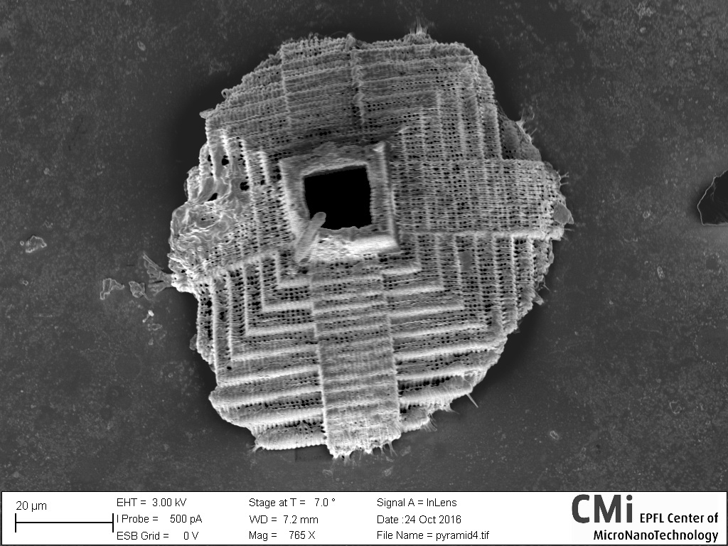
The return of Quetzalcóatl
Edgar Emilio Morales Delgado, LAPD
The latest invention I have conceived during my doctoral studies at EPFL is the world’s thinnest 3D printer. Using two-photon polymerization, this replica of the Temple of Kukulcán in Chichén-Itzá, México, was fabricated through a multimode optical fiber as thin as a couple of human hairs. The base and height of this micro pyramid is 100 and 50 µm respectively. The lateral resolution of my printer is 500 nm. This picture was taken with the SEM at CMi.
2016, September
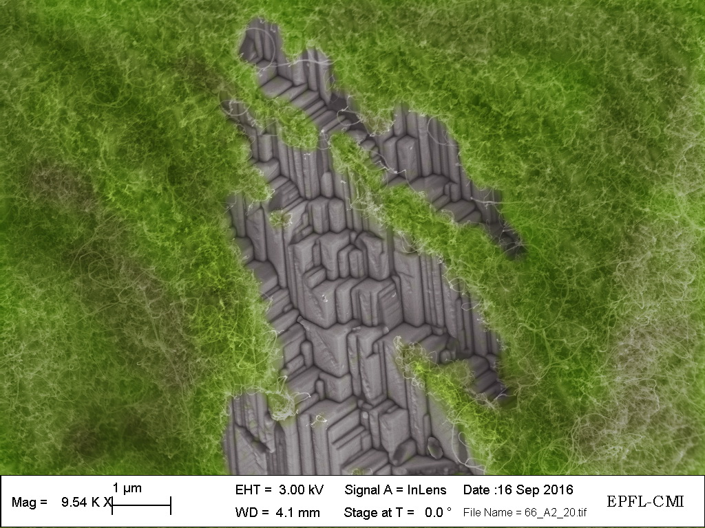
A stroll in the village of Vik
Reza Soleiman, POWERlab
This image, beautifully resembling a basalt cliff and the tiny plants that grow between the rocks, shows a deep scratch on a GaN wafer with a layer of carbon nanotubes grown on it. The basalt cliffs exist all around the world (even in CMi!) however this SEM picture, looks like to be taken from the cliffs beside the black sand beach in Vik (Iceland).
2016, August
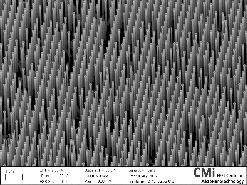
Something between us
Wonjong Kim, LMSC
Here is the SEM image of GaAs nanowires on a 4-inch Silicon wafer. Recently, we have achieved high vertical yield GaAs nanowires using pre-defined pattern hole arrays. You can see very uniform and well-ordered nanowires. Among them, we are attracted by 4 couples of wires touching each other. Although this is due to the scanning electrons, they seem to telling me that they were meant to be. Image was taken in CMi, Zone 15, SEM Merlin.
2016, July
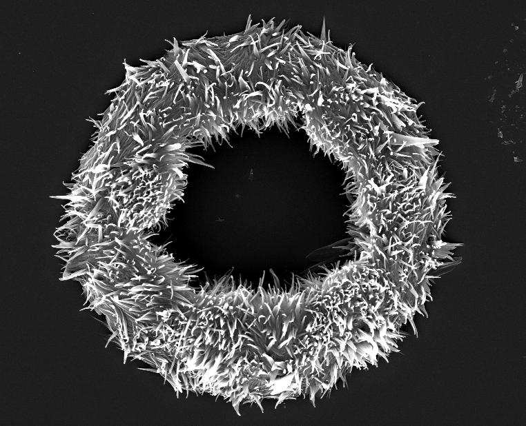
Donut of thorns
Huachuan Du, SMAL
The thorns are the NaHCO3 crystals produced by spray drying in a microfluidic nebulator. The PDMS nebulator is fabricated by soft lithography in CMI.
2016, June
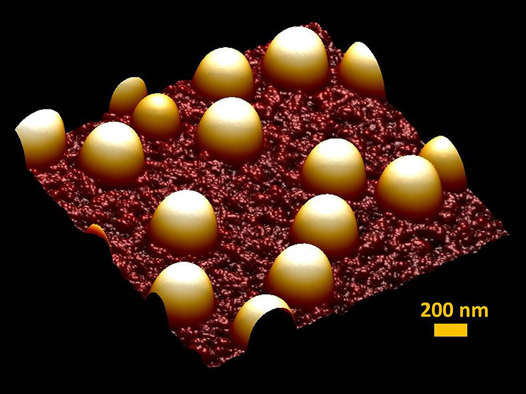
Dinosaurs are not extinct!
Wonjong Kim, LMSC
Here is the AFM image of Ga droplets on a porous silicon substrate. Porous silicon was obtained with hydrofluoric acid and nitric acid treatment. Ga droplet sitting on a porous silicon remind me of eggs of dinosaurs. It is telling me that the dinosaurs are not extinct! Image was taken in CMI, Zone 15, on Bruker FastScan.
2016, May
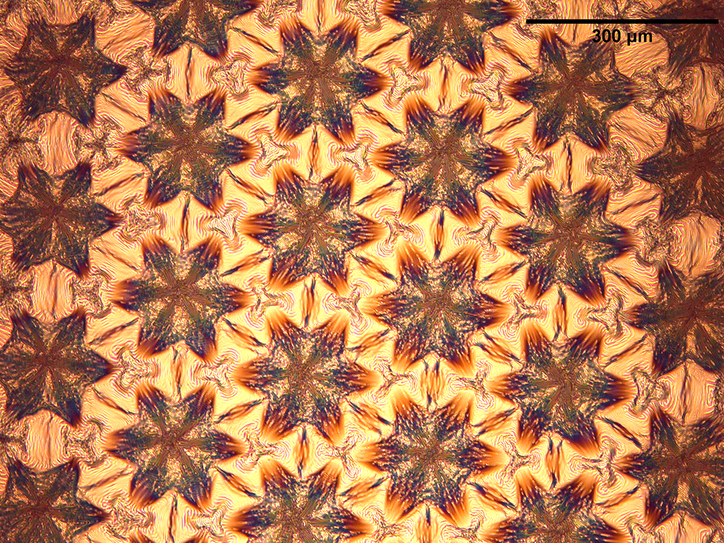
Christmas card
Marta Airaghi Leccardi, LNE
Iridium oxide was sputtered onto PDMS through a stencil mask. The star shapes are formed due to the hexagonal pattern of the circular holes in the mask and the gap between the mask and the surface of the PDMS. Imaged by an optical microscope.
2016, April
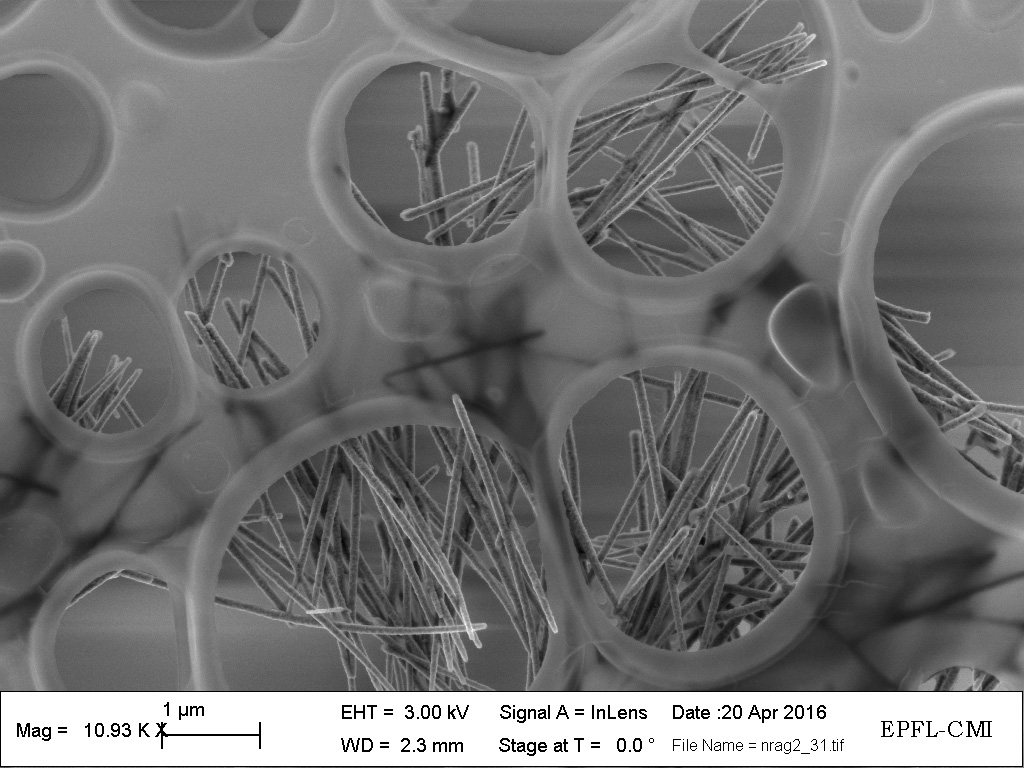
See-through
Marco Negri, LMSC
What’s behind? Using electrons, it is possible to “see” what’s behind a layer which is thin enough. In this case, zinc oxide nanorods are embedded in the carbon of a TEM grid. They are playing peekaboo through the holes in the carbon layer, but it is possible to recognize their shape even in the areas where they are covered. A relatively small acceleration voltage (3keV) is enough for the electrons to pass through the 20 nm thick carbon.
2016, March
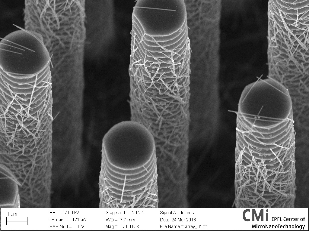
Liana around antic columns
Dmitry Mikulik, Jelena Vukajlovic, LMSC
Silicon micro pillars for solar cell applications were fabricated using phase-shift lithography and top-down etching process in CMi. On the image, you can find them as large columns with nice etching artefacts. Then, for top transparent contacts, we use Ag nanowire mesh, deposited on the sample surface using spin-coater from the liquid solution (done in Polymer Laboratory in EPFL). Thin wires of silver make continuous network, connecting all micro-pillars together. They look like liana around antic column.
2016, February
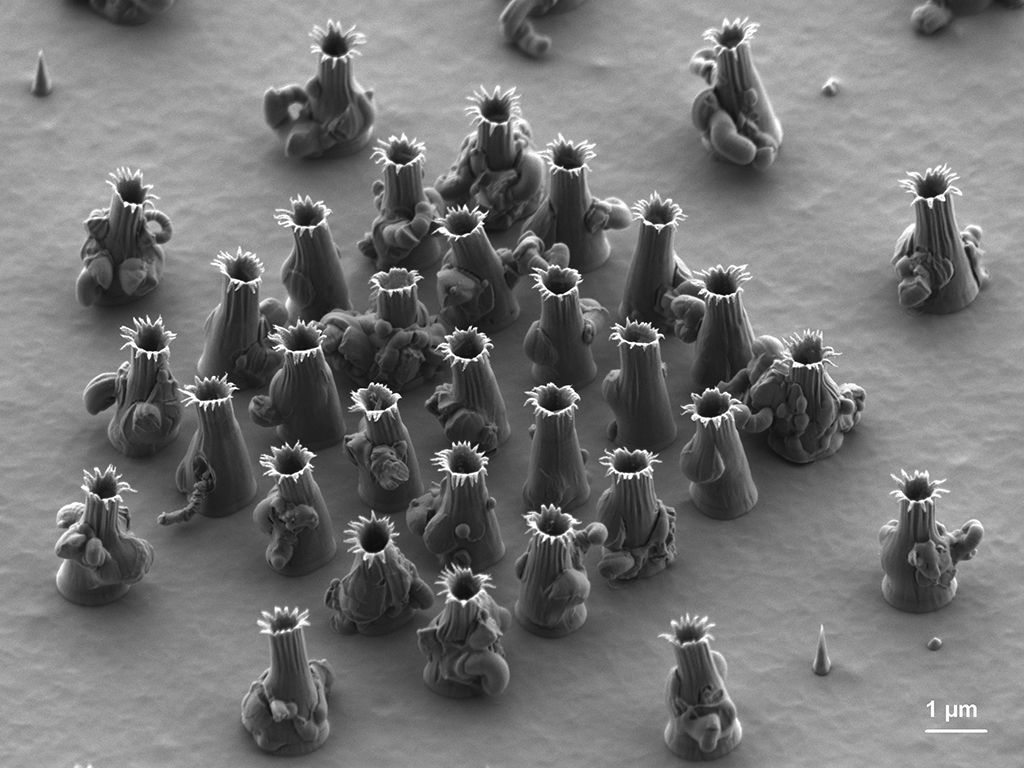
Sunflower party
Benoît Desbiolles, LMIS4
Valentin Flauraud, LMIS1
Metallic nano-flowers generated by ion beam and chemical dry etching of an Al-Ti-Au-Ti coated wafer, patterned with standard photolithography. After etching, the resist is removed, the stress in the fences is released leading to the formation of the wavy stem/leaves of the flower. The residues surrounding the base are most likely due to corrosion during chemical etching. 100% Made in CMi.
2016, January
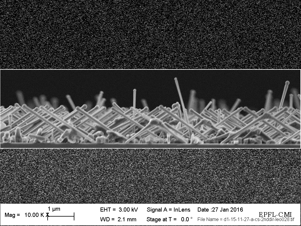
Micro-matchstick carpet
Mahdi Zamani, LMSC
Cross sectional SEM of GaAs nanowires grown on a GaAs {100} substrate, taken in direction perpendicular to the major flat of the wafer. Tilted wires with the angle of 54 degrees are of {111} direction. It is interesting to note the droplets at the top of the wires.