Coating
In CMi, the only option to coat your substrate is through spincoating.
The available spincoaters can be either automatic (cassette to cassette robot handling) or manual.
- Automatic :
+ CMi provides, qualifies, and maintains coating recipes
+ Stable process (dispense rate, dispense volume), ambiant (temperature, humidity) conditions
+ No particle contaminations
+ Edge clean, back side rinse and edge bead removal
– Only SEMI wafer 4” and 6” accepted (for non-standard substrate – see this link)
- Manual :
+ Process is fully customizable
+ Almost all substrate dimensions are accepted
+ Any chemistry/photoresists can be used (if accepted by CMi)
– Process variation
– Potential particle contamination
To decide which tool you should be using, the two main criterion are :
- Is the equipment compatible with my sample dimensions (SEMI wafer or not) ?
- Is the photoresist/polymer available for coating on the tool ?
Below is a table listing all the spincoaters in CMi and which photoresist/polymers are available on them.

Exposure
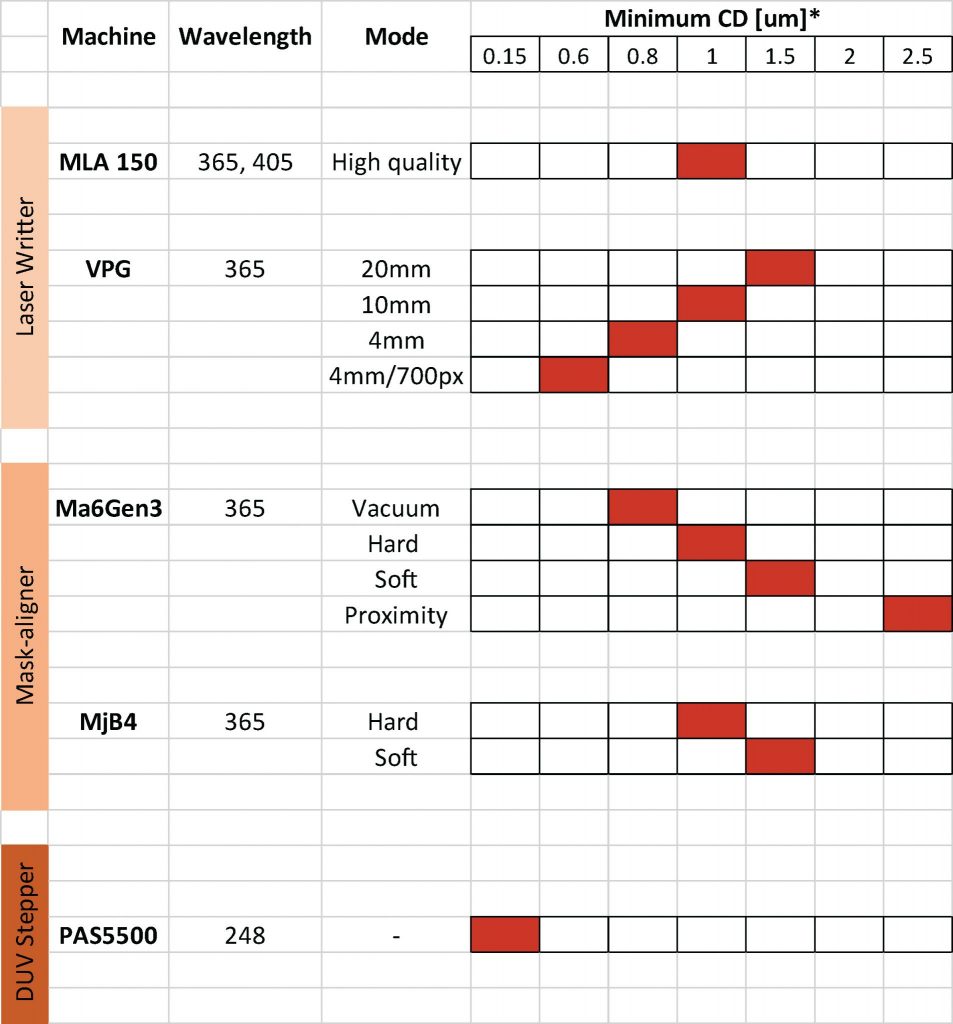
CMi offers a wide range of tools to expose your samples. Below, you will find the main pros and cons of each type of equipment, information about substrate requirements and restrictions, and a table of the ultimate patterning resolution you can achieve in optimal conditions.
- Direct laser-writer
+ The layout can be changed every exposure (no mask required)
+ Accept almost any kind of substrate shape and dimensions
– Time of exposure (~ 15-20 minutes /wafer)
– Potential stripe stitching defects
- Mask-aligner
+ Time of exposure (< 1 minute /wafer, including loading/unloading)
+ Full field exposure (no stripe / field stitching issues)
– Layout fixed with the mask
– Initial cost for the mask fabrication
- DUV Stepper
+ High resolution, down to ~150nm
+ Alignment precision and repeatibility down to ~30nm
+ Production throughput, up to 100 wafers /hour
– Expensive initial cost due to the price of 6*6 inch quartz reticle fabrication
– More substrate restrictions: 4inch only, maximum bow < 30um, low TTV
To determine which tool you should be using, the main criterion are :
1. Critical dimension
How small are the smallest features in the design. Below are presented the capabilities of each tool and their specific modes.

2. Number of samples and batches exposed with the same design
For wafers:
As a general rule, if the design layout is still a prototype and changed at every exposure session, then it is advantageous to use a direct laser-writer equipment.
However, creating a mask becomes an option to gain some time in the following cases:
- The user exposes batches of wafers (more than 5+) in a single session. Exposing a wafer with a mask takes from 5 to 30 seconds when a laser-writer exposure will last around 15 minutes per wafer.
- The use exposes thick photoresist (Su8, AZ 40XT, …) requiring extremely high doses (>500 mJ/cm2). In that case the exposure duration for a single wafer can extend to more than 1 hour.
On the other hand, if the design layout is optimized and final and a high number of wafers are going to be exposed, using a mask-aligner (and fabricating a chrome mask) will be much more efficient.
For chips:
Users working with small samples (less than 2 x 2 cm2) can work with a laser-writer no matter the number of samples & exposure sessions. Since the exposure duration with a laser-writer is proportional to the sample area, chips are usually exposed in a very short time (~ 1-2 minutes).
3. Sample dimensions and properties
Laser-writer
- MLA150
- Free shape (min : 5x5x0.1mm / max : 200x200x12mm)
- VPG200
- Wafers: 4″ – 6″ (cassette loading), 8″ (manual loading)
- Masks: 4″ – 5″ – 7″
- Reticles (DUV stepper): 6”
- Chips embedded in carrier wafer (how to : here)
Mask-aligner
- Various chucks allows to expose on wafers (up to 6”) and chips of any size. However, the critical dimensions that can be reached are worse on chips than standard wafers.
DUV stepper
- Standard 4” SEMI wafers only with restrictions on their properties (bow, TTV). Please contact the photolithography staff for more information.