Table of content
- Photolithography Inspection
- Photolithography Rework
- Descum before processing
- Stripping after processing
Photolithography inspection
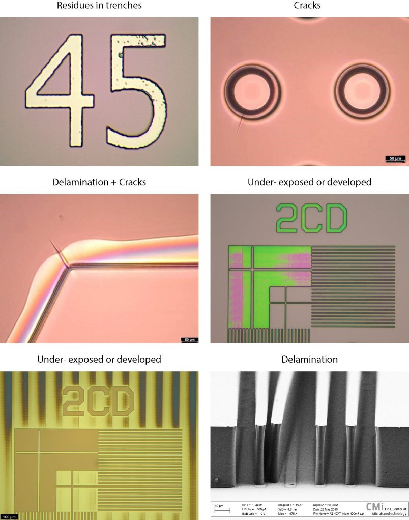
It is strongly recommended to inspect the wafers at each step of the photolithography process and, in particular, the outcome of the patterning process after the development, before moving on the next step of the process flow.
Photolithography is not irreversible and wafers can be easily reworked in case of patterning issues! On the contrary, when the substrate has been etched or a thin film deposited, it is generally too late to recover the wafer.
Make sure to use the optical microscopes available in almost all zones of the cleanroom, save images and contact the photolithography staff for advice.
The user must ensure that :
- Before the exposure:
- Coating quality is good enough for the planned lithography (100% wafer coverage, visually uniform thickness (color), minimal ammount of particle defects, etc..)
- The PR layer is thick enough for the successive process
- After development:
- The dimensions of the pattern are respected
- The development is complete, i.e. no undesired resist leftovers
- The photoresist has not delaminated from the substrate
In the case of incomplete development, due to insufficient exposure dose or development time, it is advised to perform at least one more development run in order to clear the remaining photoresist from the surface before. If the development is still not complete after 2-3 development sequences, then the resist should be stripped.

Photoresist stripping for photolithography rework
If the photolithography inspection highlight some issues after coating or development, it is generally possible to strip the resist and redo the lithography.
CMi recommends :
- O2 plasma asher (only for PR layer <8um):
First, make sure your sample is accepted in the machine ! Metals such as Au, Ag, Cr, Cu, Fe are usually not welcome.
- Solvent (NMP) wet chemistry:
- UFT resist (Z2)
HMDS is not fully removed in solvent wet chemistry. If possible, it is advised to perform a short cleaning in a plasma asher, typically Tepla (Z1 or Z11) – 5 minutes high power. Alternatively, users can immerse the wafers in a standard PR developer (AZ 400K, AZ 726 MIF) for a few minutes. Developers are available on the Arias base bench (Z13).
Special cases & alternatives
- SU8
- unexposed: can be dissolved in PGMEA (rinse : IPA + DI) on the Arias solvent bench (Z13)
- exposed: can’t be stripped
- Polymide
- soft-baked: can be dissolved in NMP (rinse : IPA + DI) on the UFT Resist (Z2)
- full-cured: possible to remove in a oxygen plasma
- Cyclotene BCB
- soft-baked: can be dissolved with Rinse T1100 (rinse : IPA + DI) on the Arias solvent bench (Z13)
- full-cured: possible to remove in a oxygen plasma
Surface cleaning before a process step (descum)
If the photolithography inspection does not reveal any issues, it is still recommended to perform a short plasma O2 cleaning of the surface (descum) before moving to the subsequent step (etching or thin film deposition).
Indeed, after development, it is common that some by-products of the photoresist dissolution remains on the surface, typically in trenches and holes. These residues might not be visible with an optical microscope. If they are not removed, the device performances may be affected by uniformity and reproducibility issues.
Photoresist stripping or lift-off after a process step
Removing the photoresist after etching or thin film deposition can sometime be more tricky than after coating since the PR can sometime be slightly burned or damaged from harsh process conditions. The following section give process recommendations for:
- After etching (wet / dry)
- After thin film deposition (lift-off)
1. After etching
1.1 wet-etching
In most case, the photoresist is not particularly harmed by the etchant.
CMi recommends :
- UFT Resist (Z2): Remover 1165 (NMP chemistry)
1.2. dry-etching
Depending on the plasma condition (chemistry, duration, etc..), the surface of the photoresist undergoes a transformation during the etching process that makes it harder to strip. It is important to weaken this layer to fully remove the photoresist.
CMi recommends :
- Tepla GIGAbatch (Z1), or Tepla 300 (Z11): 5 minutes – High power
- UFT Resist (Z2): Remover 1165 (NMP chemistry)
If not successful, severely burnt resist can potentially be cleared with the following solutions, available in Zone 13:
- Arias Base (Z13): Technistrip P1316 for positive photoresists
- Arias Solvent (Z13): Technistrip Ni555 foe negative photoresists
2. After thin film deposition (Lift-off)
The result of the liftoff depends mainly on the photoresist type, thin film deposition method and design geometry.
For lift-off in cassette
- Plade Solvent (Z1): SVC14 – IPA – DI water
- Wafers (4” and 6”) and small samples – list of available holder
- Ultrasonic agitation
Single beaker or chip lift-off
- Arias Lift-off (Z12), Remover 1165 / SVC14 / Acetone – IPA – DI water
- Wafers 4” and small samples
- Ultrasonic agitation
- Heating
Both Remover 1165 (NMP) and SVC 14 (DMSO) are suitable to completly remove photoresist.
NMP have been classified as reprotoxic, the CMi strongly recommends to use SVC 14 since performance are comparable.
Applying ultrasonic agitation and warming up the solution can shorten the lift-off duration and increase the chance of success.
