Selecting the right photoresist (PR) is crucial for achieving precise and reproducible results in photolithography processes. For each process step, the selection involves considering factors such as resolution, sidewall verticality, etching resistance & selectivity, and compatibility with the substrate topography and material.

Resist table
Here is a summary of the photoresists available in CMi with information on their thickness range and the minimum critical dimension that can be achieved (in ideal conditions).
More details can be found here : Photoresists available in CMi
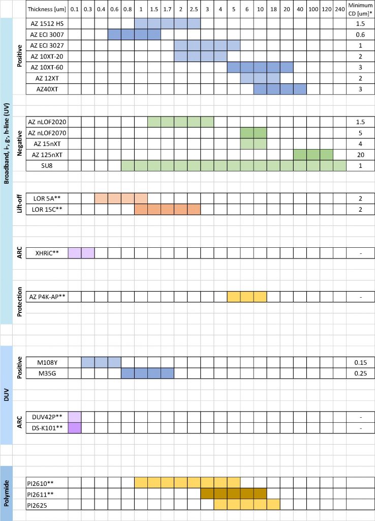
** : Non-photosensitive
Process steps
Below is described the main criteria for choosing the appropriate photoresist based on the succesive step in the process flow.
Critical dimension down to 600nm (i-line)
The minimum dimension that can be printed with photolithography depends both on the photoresist properties (thickness, sensitivity,…) and the exposure equipment. Photolithography at the i-line (365nm) node usually start to struggle when the CD approaches 1um.
Users that want to push the resolution should make sure to use a high resolution thin photoresist (AZ ECI 3007) together with the exposure equipment with the highest resolution potentials (VPG200).
The use of a bottom anti-reflective coating (BARC) layer is also greatly recommended as it will help to reduce standing wave roughness on the resist sidewalls and stabilize the exposure parameters (less effect from the subsrate material and from PR thickness change).
Recommended Photoresist/BARC
- AZ ECI 3007
- XHRiC + AZ ECI 3007
Critical dimension down to 150nm (DUV)
DUV photolithography is available in CMI with a dedicated coating/development equipment (TEL Act 8) and a DUV stepper (ASML PAS 5500/350C) in in-line configuration. DUV has the potential to push the resolution down to ~150nm but presents several challenges compared to i-line photolithography:
- Compatibility only with 100mm wafers
- Wafer bow < 30um
- Wafer TTV < 2um (or as low as possible)
- Limited PR thickness range (selectivity issues, hard-mask may be required)
- Expensive 6inch quartz reticle
Two different photoresist from JSR are available : the high resolution M108Y that can print down to 150nm, and the slightly thicker M35G that can reach 250nm.
A BARC layer is greatly recommended to improve the uniformity and reproducibility of DUV lithography processes, but not strictly required.
Recommended Photoresist/BARC
After patterning the PR, a thin film of the desired material is deposited over the entire substrate. The PR is then dissolved in a solvent/remover, lifting off the material deposited on it and leaving behind the desired pattern on the substrate. It is commonly used to deposit metals and other materials that do not etch well. The critical part of the lift-off process is the access of the remover to the PR to remove it from the masked area.
Deposition with a thermal or electron-gun evaporator
If the deposition is uni-directional (i.e. using an evaporator), the following is what it will look like for positive and negative PR :
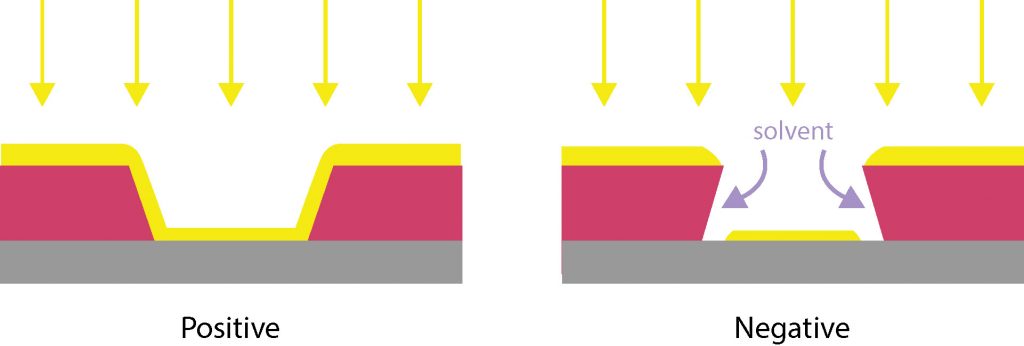
As one can see, the negatively sloped sidewalls have shadowed themselves from the deposition and will be accessible to the remover.
Another option is to use a sacrificial layer under a positive PR layer to create an undercut. This sacrificial layer does not need to be exposed; it will be etched by the developer. The development time has to be adjusted according to the desired undercut.
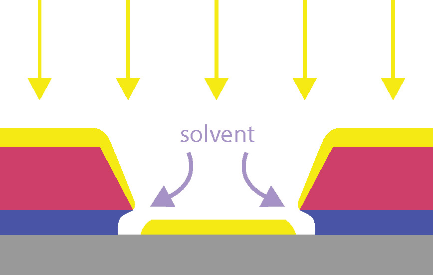
As a rule, one should never deposit more than 1/3 of the sacrificial layer thickness to get good lift-off results.
With LOR 5A, the maximum thickness deposited is <300nm, while LOR 15C will allow thickness deposition up to 1um.
Negative photoresist of the nLOF family are thicker and have better thermal resistance. In consequence they can potentially be used to deposit thicker metal stacks, up to several microns when using AZ nLOF 2070.
Recommended photoresist
- AZ nLOF 2020 (negative)
- AZ nLOF 2070 (negative)
- LOR 5A + AZ 1512 HS (positive)
- LOR 5A + AZ ECI 3007 (positive)
- LOR 15C + AZ ECI 3027 (positive)
Deposition with a sputtering equipment
In practice, many materials are not available in the evaporator system, or some users may wish to use sputtering deposition for specific reasons. In this case, it has been shown that using a positive PR with almost vertical sidewalls can work for the lift-off process.
The use of a heated remover (~80°C) and ultrasonic agitation will help to crack the thin film deposited along the sidewalls to allow the remover to access the PR. In this case, the lift-off process will be much longer and may not be successful. Also the resulting metal pads will show uneven and unsmooth edges.
Recommended photoresist
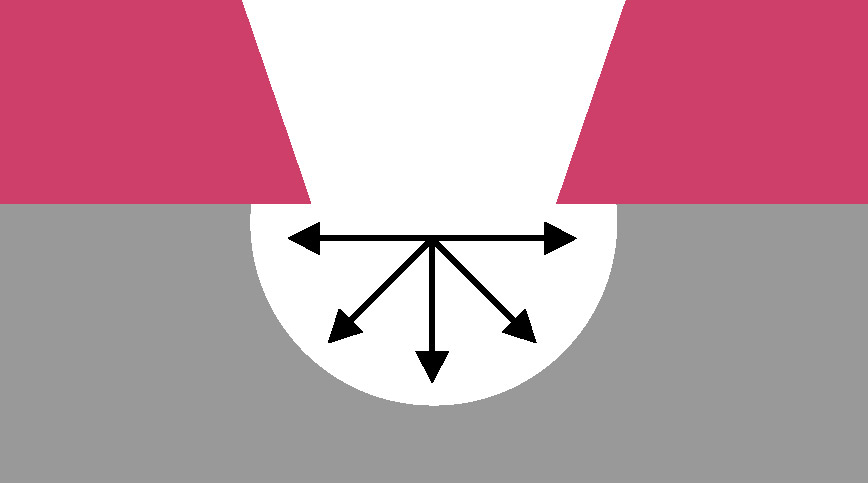
Due to its isotropic behaviour, wet chemical etching requires optimal adhesion to the substrate to reduce the amount of lateral under-etching.
Wet etching is extremely selective and, since the photoresist is barely attacked, it is usually better to use a thin low-stress photoresist. Photoresists that do not have a required post-exposure bake (PEB) step are preferred.
Recommended photoresist
Ionized gases or plasmas are used to selectively etch material from a substrate. Plasma chemistries are mainly based on fluoride (C4F8, SF6, CF4, CHF3), chloride (Cl2, BCl3) or bromide (HBr) compounds involving ions with very high electronegativity. The plasma chemistry, as well as the acceleration voltage will affect the etch selectivity between the substrate material and the photoresist mask. Users should make sure to choose the photoresist thickness that will be sufficient to reach the target etching depth.
Shallow silicon etching :
Shallow etching is mainly focussed on pattern transfer fidelity and smooth sidewalls
Recommended photoresist
Deep silicon etching (Bosch process) :
The profile of the PR sidewalls will have a major impact on the final result. In general, the sidewalls should be as vertical as possible.
Recommended photoresist
- AZ 12XT
- AZ 40XT
- AZ 10XT-60 + overnight hardbake @85°C
Dielectric etching
Process to etch dielectric are quite aggressive. Good resistance and high softening point at higher temperature are required.
Recommended photoresist
- AZ ECI 3007
- AZ ECI 3027
- AZ 10XT-60 + overnight hardbake @85°C
- AZ 15nXT
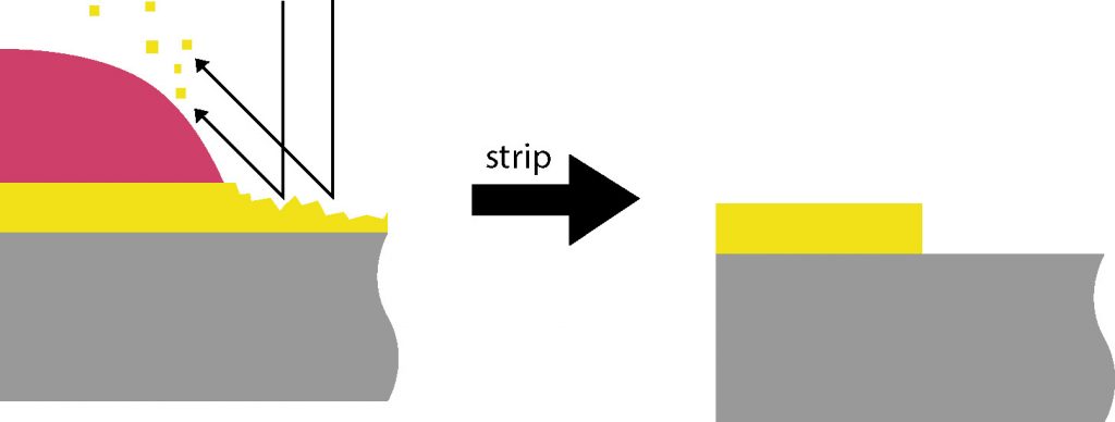
Ion beam etching is a technique that uses a focused ion beam (e.g. Ar) to remove material from a substrate. Special care must be taken to avoid any redeposition of the material on the sidewalls of the PR which will lead to fence formation as shown below.
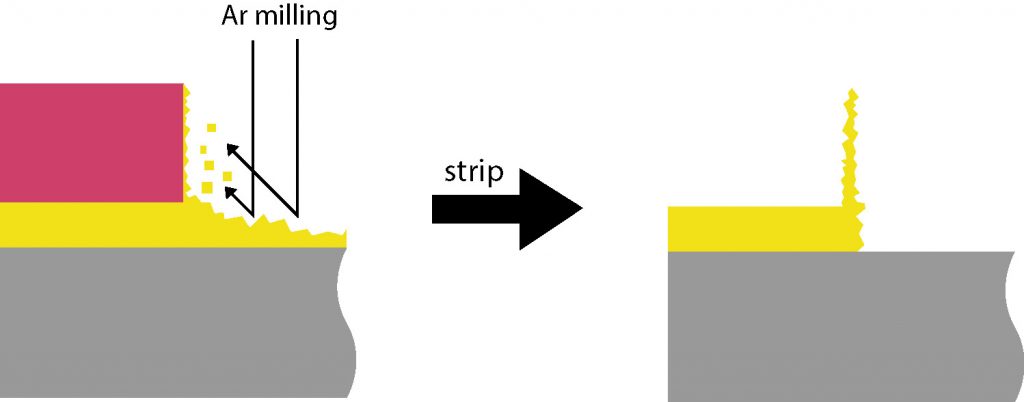
To avoid this issue, the sidewalls slope can be decreased through a reflow process (i.e. heating the PR above its glass transition temperature for an extended time). Not all PRs are suitable for this process. With rounded flanks, redeposition will be minimal.
Recommended photoresist
Dicing is a “dirty” process that creates a lot of dust and debris. It is recommended to deposit a protective coating to keep the surface undamaged and free of particles.
AZ P4K-AP is used in CMi as a protective coating for dicing. The polymer is not photosensitive and therefore cannot be exposed to be patterned. For adequate protection, make sure to coat a layer thicker than your highest topography.
Recommended photoresist
A mold to be used with PDMS must have high solidity and, if it consists of a patterned resist, good adhesion between the resist and its substrate to be able to withstand multiple molding/demolding operations
There are three main way to create a mold for microfluidics at CMi :
SU-8 lithography
+ Only one lithography step
+ Smooth sidewalls
+ Multilayer possibility
– More restriction on aspect-ratios
– Fragility
Recommended photoresist
Dry-Etching
+ Solidity
+ Aspect-ratios
– Sidewalls roughness when using Bosch process
– Require : lithography + etching + stripping
– Uneven etching depth (dependant on aspect ratio)
Recommended photoresist
- AZ 12XT
- AZ 40XT
- AZ 10XT-60 + overnight hardbake @85°C
Positive photoresist
+ It can be reflowed to obtain semicircular channels
+ Smooth sidewalls
– Limited thickness range and aspect-ratios