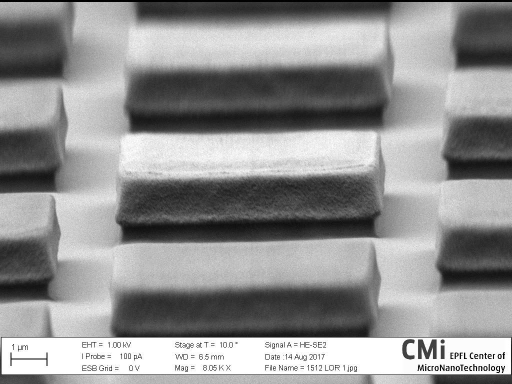
LOR 5A (Lift-Off Resist) is a polymer which dissolve in alkaline solutions. LOR 5A, used as sacrificial material, can be underetched with standard photoresist developers (TMAH- or KOH-based) just by extending the development time of the imaging top resist. This method is known as the double layer lift-off or bi-layer lift-off. Extreme resist profile can be obtained, enabling efficient lift-off of evaporated or even sputtered material.
- Coating Tools : EVG 150; Sawatec SM-200
- Thickness range [µm]: 0.4 … 1
- Minimum CD / typical aspect ratio: ~ 2um
- Substrate topography: Planar or very low
- Recommended for: Lift-off
Process in CMi
! Cleanroom humidity warning !
Control of the relative humidity (RH) in photolithography zones is extremely critical. Stable and reproducible photolithography is expected within 38% to 48% RH range.
- In case of low RH (< 38%), the resist sensitivity and development rate decreases. It is then recommended to increase the recommended exposure doses.
- In case of high RH (> 48%), the resist adhesion decreases. It is then recommended to do an additional bake (>10 minutes @ 150°C) before loading the wafers in the HMDS or coating equipment.
Wafer surface preparation
When used as recommended, primers such as HMDS are typically NOT required to promote the adhesion of LOR products.
Assuming wafers with clean surface without organic contamination, good adhesion of the LOR 5A polymer is observed with the following surface treatments:
| Surface material (larger area) | Vapor HMDS | Plasma O2 | Thermal dehydratation |
|---|---|---|---|
| Si | √ | √ | √√ |
| SiO2, fused silica, SiN, Si3N4 | √ | √ | √√ |
| Float glass, pyrex | √ | √ | √√ |
| Metals: Al, Au, Pt, Ti | … | √ | √√ |
| Metals: Ag, Cu, Cr, Fe | … | X | √√ |
| III/V semiconductors (GaN, GaAs) | … | X | √√ |
Legend: √√ Strongly recommended / √ Alternative process / … Not effective / X May affect or destroy underlaying material
Spincoating
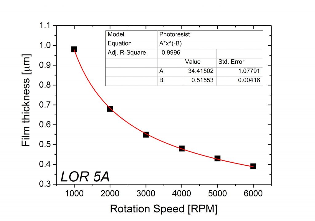
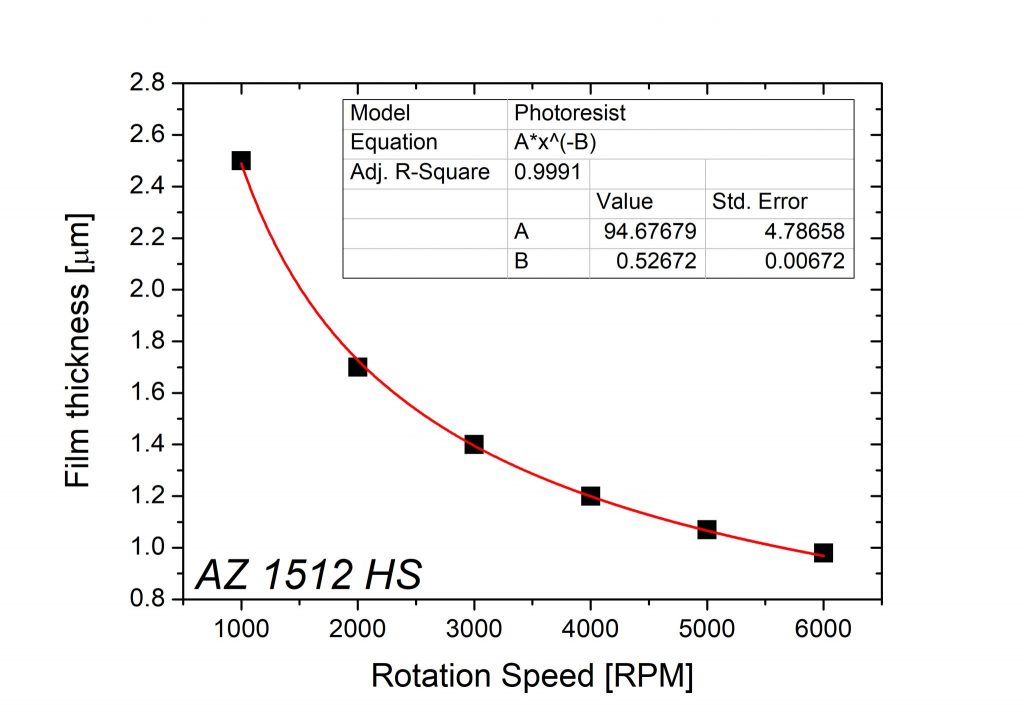
The LOR 5A and AZ 1512 HS spincurves are shown below, as well as process details for both automatic and manual coating.
Available thicknesses:
- option 1: LOR 5A 400nm + AZ 1512 HS 1.1um (metal stack < 150nm)
- option 2: LOR 5A 700nm + AZ 1512 HS 1.6um (metal stack < 300nm)
Available databases:
- Lift-Off_LOR_Std_Dehydrate_x_y
- Lift-Off_LOR_Std_NoDehydrate_x_y
- Lift-Off_LOR_GlassOnly_Dehydrate_x_y (for transparent wafers)
- Lift-Off_LOR_Quartz_Dehydrate_x_y (for quartz, stacked glass-silicon wafer or SOI wafers. Softbake temperature for AZ 1512 HS is 105°C)
Available recipes:
1st layer, LOR 5A:
| Recipe name | Spin speed [rpm] | Cure time [mm:ss] | LOR thickness [µm] |
|---|---|---|---|
| C4_D_LOR_u4_EC | 6500 | 04:10 | 0.39 ± 0.2 |
| C4_D_LOR_u7_EC | 1200 | 04:10 | 0.73 ± 0.3 |
Spin time is 25s. Bake over material glass transition at 375µm proximity gap. Cure temperature is 190 °C for 250 s.
Note: LOR 5A is very stable. Wafers can be prepared several days in advance.
2nd layer, AZ 1512 HS:
| Recipe name | Spin speed [rpm] | Cure time [mm:ss] | LOR thickness [µm] |
|---|---|---|---|
| C4_N_1512_1u1_EC | 6000 | 01:30 | 1.1 ± 0.1 |
| C4_N_1512_1u6_EC | 2800 | 01:30 | 1.6 ± 0.1 |
Spin time is 30s. EBR and BSR cleanning options. Softbake at 240µm proximity gap. Softbake temperature is 100°C for 90 s.
Combination LOR 5A + AZ 1512 HS (not recommended):
| Recipe name |
|---|
| C4_LOR_u4_1512_1u1_EC |
| C4_LOR_u7_1512_1u6_EC |
- Find the spin-coating speed “XXXX” [RPM] matching your target thickness from both the LOR 5A and the AZ 1512 spincurves.
- When coating on wafers, use the STD_”XXXX” recipe, which includes a 500 RPM spreading step and 40 seconds of main coating step.
- When coating on small chips, use the CHIP_”XXXX” recipe, which includes 40 seconds of main coating step and a short acceleration at the end to reduce edge bead effects.
- LOR 5A cure temperature: 180°C (Use the Z13 Euroterm hotplate SP=197)
- LOR 5A cure time: 4’10”
- AZ 1512 HS softbake temperature: 100°C (Use the SSE SB20 hotplate SP=106)
- AZ 1512 HS softbake time: 1’30”
Exposure
The following table lists the recommend dose “to clear” for LOR 5A / AZ 1512 HS double layers, coated on silicon wafers. It is recommended to perform a contrast curve / exposure matrix calibration for wafers other than silicon.
| Illumination: | Broadband* | i-line (355-365 nm) | h-line (405 nm) |
|---|---|---|---|
| Equipment: | MABA6, MA6 Gen3 (no filter) | VPG 200, MA6 Gen3 (filter), MJB4 | MLA 150 |
| PR | Dose [mJ/cm2]+ | Dose [mJ/cm2]++ | Dose [mJ/cm2]+++ |
| AZ1512 1.1um (LOR 400nm) | 40 | 42 | Refer to Resist Tables |
| AZ1512 1.6um (LOR 700nm) | 65 | 68 |
* Mercury Lamp, Mask Aligner with UV400 configuration & no filter / + Based on intensity readings from Süss optometer broadband CCD / ++ Based on intensity readings from Süss optometer i-line CCD / +++ Based on MLA150 internal dose measurements
Development
The recommended developer for LOR 5A / AZ 1512 HS is AZ 726 MIF (or MF CD 26), an organic solution based upon TMAH.
Development recipes for LOR 5A / AZ 1512 HS (identical for all are Lift-Off_LOR_* databases) are listed below:
| Recipe name |
PR thickness [µm] |
Total contact time [s] |
|---|---|---|
| D4_HB_1512_1u1_PUD | 1.1 + 0.1 | 50 |
| D4_HB_1512_1u6_PUD | 1.6 + 0.1 | 75 |
Post-development bake at 100 °C for 1 min.
Development sequences for LOR 5A / AZ 1512 HS double-layers are listed below:
| Recipe name |
PR thickness [µm] |
Total contact time [s] |
|---|---|---|
| D4_HB_1512_1u1_PUD |
1.1
|
~66
|
| D4_HB_1512_1u6_PUD |
1.6
|
~100
|
For development, puddle method is used with intermediates spin-clean steps and a final spray development step. Hardbake of the resist is applied after the development, at 100°C for 2 minutes to improve the stability of the positive resist.
- Recommended developer: AZ 726 MIF (no dilution needed)
- Development time: 30″/um (minimum) + 30″ (undercut)
- Rinse: H2O 1min
IMPORTANT:
After development, it is mandatory for wafers to go through an additional rinsing step with DI water to avoid backside contamination and damage on equipments (chuck in etcher) in further processing steps. The water baths of the following wet benches can be used free of charge (5 min. billing delay after login):
- Z01 – Plade “Solvent” wet bench
- Z02 – UFT “Resist” wet bench
