


The Sample Preparation Lab is equipped with a diverse range of tools for etching, polishing, and cutting crystals with precision. The facility ensures meticulous preparation to achieve optimal surface finishes and dimensions for each crystal.
Contact:
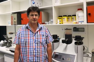
Gérald Beney
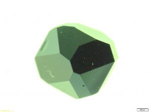
Example of preparation of a (110) oriented lamella of Cu₂OSeO₃ with 4nm surface roughness
 |
 |
 |
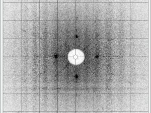 |
To prepare a thin lamella oriented along a specific crystallographic plane, the process begins by glueing the crystal to a polishing head along the selected facet of the crystal. The precise crystallographic plane is then determined with the help of a Laue camera and a goniometric head that is compatible with the polishing head.
 |
 |
 |
 |
After the crystal is cut parallel to the desired crystallographic plane using a disc saw, the thin lamella undergoes polishing. This process can reduce the surface roughness to just a few nanometers. X-ray diffraction analysis confirms that the lamella remains undamaged throughout the glueing, cutting, and polishing stages.